21
\$\begingroup\$

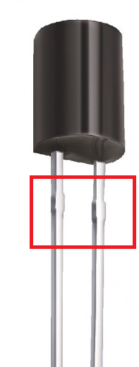
I am using an IR LED and a photo diode, and I have designed the PCB according to the specifications that I found on the datasheet - i.e. hole sizes for the pins being 0.6 mm. However, on these components there are 'knuckles' (see below image) and these are wider than the hole size they quote for the pins.

Enter image description here

So the issue is the component doesn't go low enough into the board because of these knuckles. Why are they there? How can I know how wide they are in order to make my holes account for this?

\$\endgroup\$
7
  • 1
    \$\begingroup\$ What is an issue for you, is a convenient feature for others. \$\endgroup\$
    – PlasmaHH
    Commented Apr 29, 2015 at 12:50
  • 1
    \$\begingroup\$ Is there a particular reason why you want the device flush against the PCB? \$\endgroup\$ Commented Apr 29, 2015 at 12:50
  • 2
    \$\begingroup\$ @IgnacioVazquez-Abrams Not quite flush against it, just a little lower than these knuckles - because of the shape and size of the moulding that has to fit around it \$\endgroup\$
    – MrPhooky
    Commented Apr 29, 2015 at 12:53
  • 1
    \$\begingroup\$ So make the holes bigger next time and file off the nubs (knuckles) for this one. \$\endgroup\$ Commented Apr 29, 2015 at 13:13
  • \$\begingroup\$ @GeorgeHerold Yeah but how much bigger? I don't want them to just fall through willy nilly... is there a standard size for these tabby things \$\endgroup\$
    – MrPhooky
    Commented Apr 29, 2015 at 13:20

3 Answers 3

41
\$\begingroup\$

I have two possible explanations:

  • The 'knuckles' are there intentionally to avoid the pins going all the way through the PCB.
    Most of the times it is not desired that the pins are going all the way through the PCB.
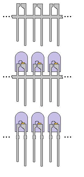
  • They are a remnant of the production process (see picture below).
    First the pins are a part of one single metal sheet and are cut after the dies and the casings are added. The cutting leaves the knuckles.

enter image description here

\$\endgroup\$
7
  • 2
    \$\begingroup\$ Nice graphics! Did you make that yourself? \$\endgroup\$
    – sleblanc
    Commented Apr 29, 2015 at 16:25
  • 25
    \$\begingroup\$ @sebleblanc: yes, with MS Paint :-) \$\endgroup\$
    – Curd
    Commented Apr 29, 2015 at 16:48
  • \$\begingroup\$ Also, they might help keep the led on the board. At least when soldering manually, I've noticed that they keep the led from falling from the board until I solder it. \$\endgroup\$
    – Paul92
    Commented Apr 29, 2015 at 21:32
  • \$\begingroup\$ @Paul92 But for that, you can slightly bend the LED leg a little, so it doesn't fall straight. And somewhere I saw a question with such bent legs on the LEDs. \$\endgroup\$ Commented Apr 30, 2015 at 10:46
  • 1
    \$\begingroup\$ Nice graphics, but somewhat misleading overall in practice, alas. "Most of the time that's not desired" is ambiguous and aslight change in wording may help. ie Do you mean 'going through' or 'not going through' is not desired? \$\endgroup\$
    – Russell McMahon
    Commented May 6, 2015 at 2:35
10
\$\begingroup\$

Those particular leads in the photo do not look like they're intended to stop the part from going down as far as you like. Are you sure you used the recommended hole size in the datasheet? Or did you just take the nominal dimension and use that.. I would expect the recommended size to be relatively large for such an item.

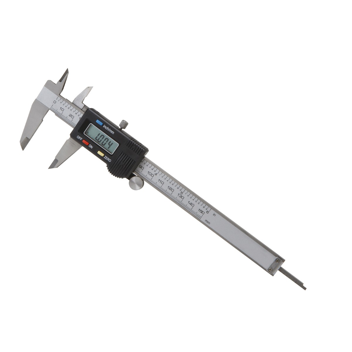
Get a set of these generic Chinese-made calipers (they're only about $10-$30 depending on where you buy them and quality). You can get higher quality ones (eg. Mitutoyo or Brown & Sharpe) but it's not really necessary and even the most expensive calipers are not suited for high precision of better than a couple thousandths of an inch (but that's good enough for drilled hole sizes).
enter image description here

You can also get a 1" micrometer if you need to measure things like thickness more accurately. The vernier type is cheap, electronic digital types still cost a bit more than mechanical types.

It's usually bad form to shove plastic molded bits right down to the board- there will be a differential CTE (coefficient of thermal expansion) between the X-Y of the PCB (small) and the epoxy (large) so that the part will be under stress and will tend to split open when exposed to temperature extremes. Allowing a bit of lead in there supplies some "give" so the part is not destroyed.

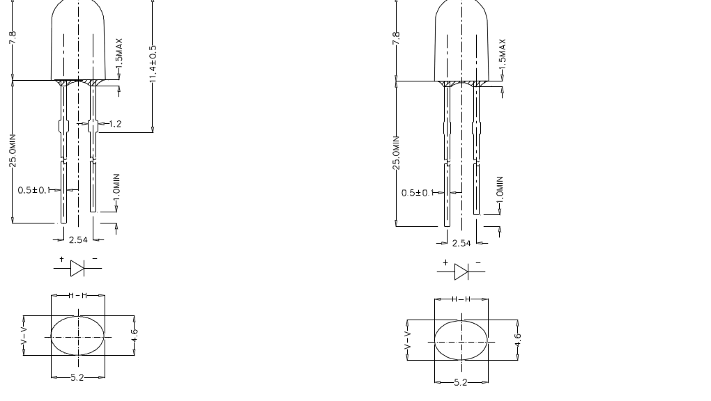
Edit: There is no shortage of poorly specified LED drawings- even from relatively well-known makers. For example, here is a fairly good one from Cree.
enter image description here

You may note that there are two lead frame variations, one with and one without the "knuckles" (as Russell mentioned in his answer), however the one without still has artifacts where the joiners from the continuous leadframes were punched out (as Curd mentioned). Unfortunately, the artifacts are not dimensioned either in size or position (and one might assume that they fit within the tolerance of the leads 0.5+/-0.1mm but I seriously doubt that is guaranteed to be true). The ones with larger knuckles have only a nominal dimension of 1.2mm, so we don't really know if a 1mm hole (for example) will allow the LED to pass through or not. The first shipment might be find and the next not, and there's no complaint one could make from the specs. Chances are a hole of 0.8mm would work, but there are no guarantees. I have other paper datasheets from really major Taiwan-based suppliers that are no better (and some are worse). The best you can do as a small quantity user is to employ the calipers (see above) on a sample and hope they don't change leadframe suppliers etc., or switch to a supplier with tighter specs.

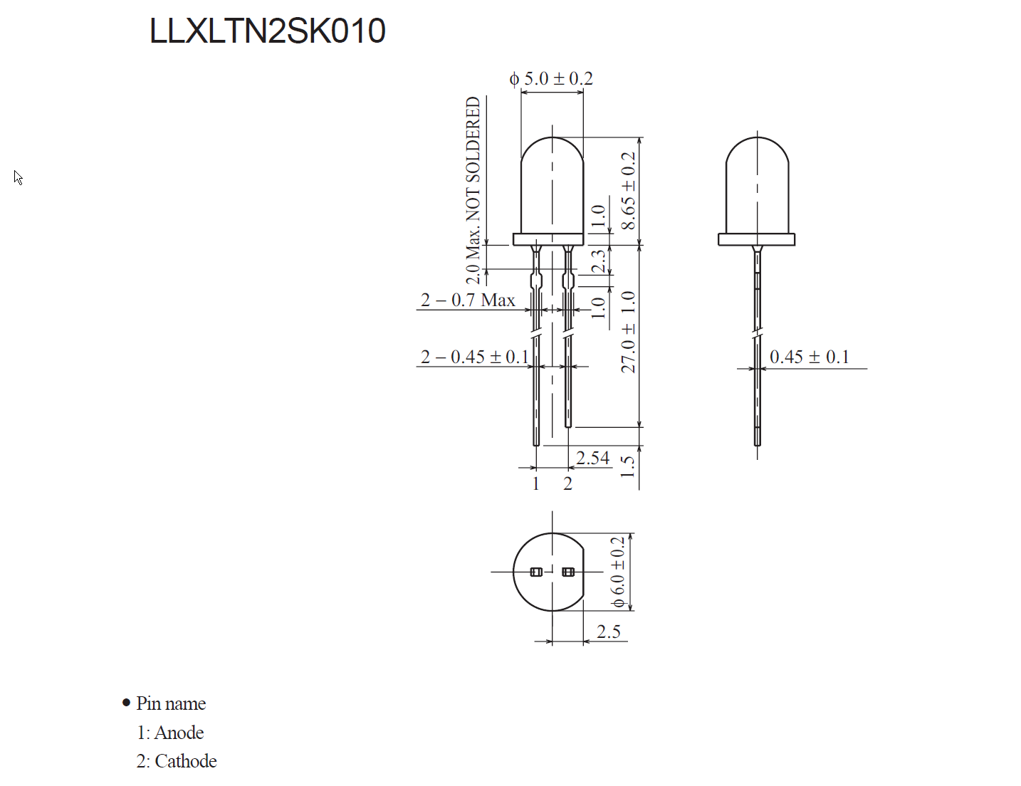
Below is a much more tightly specified datasheet drawing (from this Panasonic datasheet) that tells you all you need to know:
enter image description here

I believe that the "knuckles" here (as I opined on yours) are not intended to stop the LED from going down as far as possible- they're just artifacts of the manufacturing. The maximum dimension is specified, but no minimum, so there is no guarantee. However, there's a 2mm spec that indicates that a 2mm spacing is required under the LED (at least that's my interpretation- that it's a minimum not a maximum). This is to help keep the LED from being destroyed by differential thermal coefficients of expansion, both immediately after assembly and during operation. Note that it's above the top of the "knuckles" so it's acceptable to have the "knuckles" inside the PCB.

In general, for through-hole LEDs, we have usually used mechanical jigs to hold the LEDs relatively precisely in position during soldering, even when they are hand-soldered. If you need to get down to the 2mm-ish dimension in the above drawing, you would use a relatively large hole, so it might be sloppy depending on the LED supplier of the day. Things like cylindrical standoffs sort-of work, but they're pretty sloppy even with tight PCB through holes- the bottom of the LED is not all that flat etc. Some makers use standoffs that dissolve in the cleaning operation for crude location. Fine if you don't mind additional cost, parts etc.

Edit2: By the way, if you do decide to file the leadframe, keep in mind that you'll remove the (usually Sn) plating and expose the alloy underneath (most often it is steel to keep costs down- easily checked with a magnet). Don't expect to be able to solder to the exposed leadframe core material!
\$\endgroup\$
5
  • \$\begingroup\$ My answer may be of interest. Feel free to question any point which appears (and/or may be :-) ) off beam. \$\endgroup\$
    – Russell McMahon
    Commented May 6, 2015 at 2:33
  • \$\begingroup\$ @RussellMcMahon I generally agree with points made in your answer. I've added a couple drawings to my answer above, with bonus additional blathering. The papers or app notes on stoppers would be interesting if they are easy for you to locate. \$\endgroup\$ Commented May 6, 2015 at 10:54
  • \$\begingroup\$ Price reference for those Chinese-made calipers, I got mine, made by Shanghai Measuring & Cutting Tools Works, one of the best manufacturer of precision measurement tools in China, for US$45. It is no worse than a Brown & Sharpe's as used in my school, and it helped a lot when designing my PCB's. Cheapest option from SMCTW is US$10, same precision as a metal one, but made in plastics. \$\endgroup\$ Commented May 6, 2015 at 10:55
  • \$\begingroup\$ The one I generally use has a large yellow screen and uses a high-capacity CR2025 lithium battery, and has a nice hard case. Made by a top China factory. I think I paid around US$30 in Canada, but I know where to buy this kind of stuff. ;-) \$\endgroup\$ Commented May 6, 2015 at 12:09
  • \$\begingroup\$ The relative overall "scoring" is interesting on this one. I wonder what the lesson is ? :-). \$\endgroup\$
    – Russell McMahon
    Commented May 7, 2015 at 7:07
4
\$\begingroup\$

Summary:

While such protrusions or "stoppers" might conceivably be the result of manufacturing artefacts this is almost certainly not the case in components intended for PCB through hole insertion.

Components with or without such protrusions are available 'to order' from some manufacturers. They play a very real role in component alignment and positioning. I have a number of papers on their merits and use which I can locate and reference if there is enough interest.

Making holes large enough to allow stoppers to pass through them can lead to a range of problems.

Longer:

The "knuckles" are called "stoppers" (by at least some component manufacturers, and are intended to both allow & cause the component to sit in a fixed alignment both:
relative to the plane of the PCB and above the PCB surface.

The body moulding of components such as LEDs are less constrained dimensionally (aka built with less intended accuracy) than the frame and leads, and seating components bodies against the PCB surface will which cause greater average misalignment from the vertical. Components that emit or detect radiation may have their performance and/or appearance affected by such misalignment.

Affect on reverse side soldering would probably be minimal but may happen to some extent.
However, a component seated against a PCB will be subject to stress on the lead to body interface when radial force is applied to the top of the component. In some cases the height is much greater than the leverage arm at the board surface and "sideways" forces on the top of the component (such as an LED) may be multiplies by eg a factor of 10 at the lead-body interface.

Thermal contraction after soldering will tend to "pull the pin out of the body" if the body is hard seated against the board. Even if this does not cause noticeable short term damage there may be ongoing stress at the lead-body interface which "resolves itself" over time. Damage which results in detectable problems may be small but contribute to ongoing reliability issues.

A component seated against the PCB surface makes access to the lead-PCB intersection unavailable or less available to cleaning fluids, if used, and may also trap such fluids.


Important:

Some manufacturers specify two varieties of components which are identical apart from being supplied with or without stoppers. Designing for one type and being supplied with the other type can have a major impact on production aspects. If holes are made oversize to allow stoppers to pass through then components may end up semi-randomly misaligned after soldering. The result can look very bad in a product using eg multiple LEDs as a light source. (Ask me how I know :-) ). When soldering LEDs where alignment matters it is "common enough" to use alignment jigs to maintain alignment during soldering - with or without stoppers.

Drilling out holes or designing larger holes to accommodate stoppers so that they pass through the holes is extremely bad practice and could lead to long term reliability problems. The resultant hole to lead clearance may be significantly larger than is appropriate and may lead to solderability and soldering issues. If the components are hand soldered by people with an awareness of the practical issues and who also take proper action then problems are liable to be minimal. If automated soldering is used care needs to be taken to ensure that quality is not adversely affected.

\$\endgroup\$

Your Answer

By clicking “Post Your Answer”, you agree to our terms of service and acknowledge you have read our privacy policy.

Not the answer you're looking for? Browse other questions tagged or ask your own question.