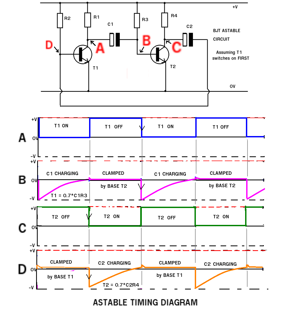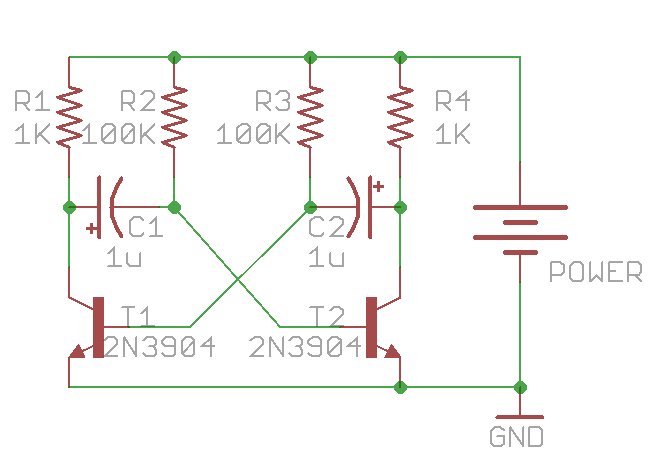
(In above timing diagram, resistors are differently numbered from OP. Following explanation uses numbers from OP. Also, in diagram, correct equation for T2 is 0.7 C2 R2 (referring to resistor numbers in diagram rather than OP).
1) Why are R4 and R1 required at all? Why would we limit current flowing into the transistors and charging the capacitors?
Transistors operate over a range of collector currents - you can look this up[ for different types (see https://www.sparkfun.com/datasheets/Components/2N3904.pdf) . The minimum values used for R1 and R4 will determine the maximum collector current. This value can easily be calculated (using Ohm's law) by assuming that all the supply voltage is dropped by the resistor. In the case of the 2N3904 the maximum current is 200mA. Failure to limit this current would damage/destroy the transistor.
The also act as part of the circuit to produce a switching voltage for one side of the capacitors
2) Why are R2 and R3 included in the circuit? It seems that they have absolutely no function.
R2 and R3 have two functions.
The first is to switch the transistors ON by connecting the bases of the transistors to the positive supply through a suitable resistor that limits the base current to a safe value.
When you first power up the circuit ONE of these transistors turns on first and start the process.
The second function is to charge the other capacitor plates attached to the bases of the transistor by connecting them to the positive supply.
When one transistor turns ON it causes the voltage at the base of the other transistor to go to a NEGATIVE voltage and turn OFF. This negative (base) voltage is also connected to the positive supply through either R2 or R3 (depending on which base we are looking at). The voltage ACROSS this resistor at this time is about TWICE the supply voltage (+V to -V). {this effect is sometimes used to produce a negative supply from a positive supply or to double the voltage of a supply}
The capacitor plate has to charge from about -V to +V and when it gets to 0.6V (just over mid way) it causes the transistor to turn ON. This is about 50% of the final voltage its trying to charge to and takes about 0.7 x time constant (either C1R2 or C2R3)
3) How are C1 and C2 discharged to allow the cycle to repeat? If they are not ever discharged, after one cycle the circuit would stop working because C1 and C2 would have a voltage high enough to limit current flow into the base of either of the transistors, effectively putting halt to the oscillations.
The trick to understanding this circuit is knowing that you can't instantly change the voltage across a capacitor.
When T1 switches ON the base of T2 is taken to a negative voltage and turns T2 OFF. The capacitor (C1) then takes time to charge back up to 0.6V through R2. When it eventually gets there (after about 0.7 C1R2) it turns T2 ON. The voltage at T2 collector suddenly drops and takes the base of T1 negative which turns T1 OFF . The capacitor (C2) attached to the base of T1 takes time to charge up through R3 until it gets to 0.6V at the base of T1 and turns T1 ON. This then results in T2 turning OFF again and the cycle keeps repeating.
The voltage at the bases of the transistor can't get higher than 0.6V because the base-emitter junction acts as a forward biased diode and clamps the voltage at that level. This ensures that the step turn OFF pulse voltage will take the base negative by about the supply voltage - 0.6V every time.


