9
\$\begingroup\$

Oldest versions of this post can be viewed through this link.

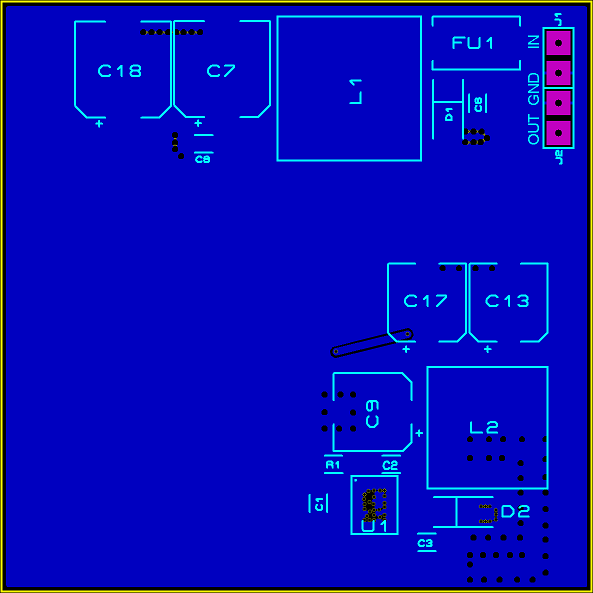
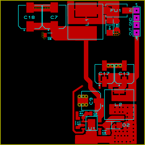
This is my re-designed layout. What is your view again?

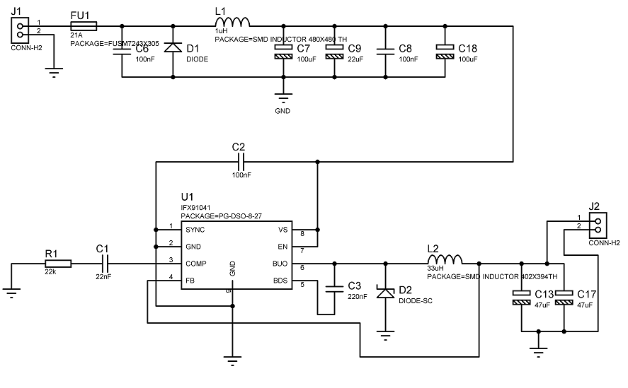
10-32V to 5V 1.2A SMPS Buck Regulator Design. The IC is IFX91041 from infineon.

Here are the schematics and layouts: http://www.mediafire.com/?69e66eje7vda1

(I was given 45 cm² (~6.98 inch²) area for both 5v 1.2A and 35V 4A.)

Schematic PCB - Top Layer PCB - Bottom Layer

\$\endgroup\$
4
  • 1
    \$\begingroup\$ Please move those images from Mediafire to our server. The question will lose a lot of value if they're deleted! \$\endgroup\$ Commented Aug 10, 2011 at 17:33
  • \$\begingroup\$ The images are already in your server, however, there are .DSN and .LYT files in Mediafire that are Proteus schematic and PCB layout files respectively. And also there is one .PDF file too. \$\endgroup\$ Commented Aug 10, 2011 at 20:30
  • \$\begingroup\$ top copper for traces on the upper area is not shown, you can refer to the .PDF file which has separate pages for separate layers. \$\endgroup\$ Commented Aug 11, 2011 at 7:37
  • \$\begingroup\$ @abdullah, if you keep editing you are not rewarding those that have already answered your questions and given improvements. Let make it multiple questions accept as you solve each step. \$\endgroup\$
    – Kortuk
    Commented Aug 17, 2011 at 13:24

3 Answers 3

7
\$\begingroup\$

I agree with the other answers here but just thought this may help:

enter image description here

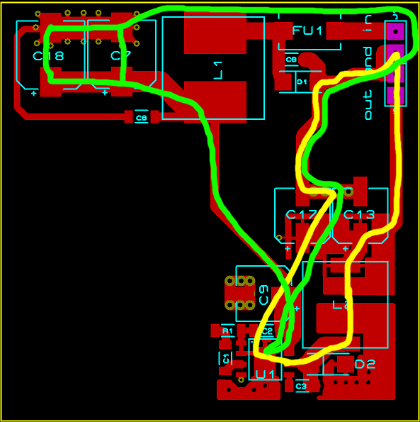
I've drawn the 2 high current / high switch frequency loops of most concern in this design.

Green shows the input current loop with the C7/C18 decoupling caps sourcing most of the high frequency current needed. This loop is very large due to poor ground design.

Yellow shows the output current loop, it is also very large.

Perhaps most concerning is that the return currents from both the input and output to the regulator share a single ground return path through the narrow trace leaving C17.

Your ultimate goal here is to minimize the loop area of both of these loops. When doing so remember that high frequency currents, those which are the EMI concern, will follow the path of least inductance to ground, not the path of least resistance.

For example, I've drawn these paths a little wide for clarity but in reality the high frequency components of the ground return path for the output current (yellow) will try to travel directly under the input current path if it can. Its more likely to bend over under L2 on its way back.

EDIT: Update for full ground plane.

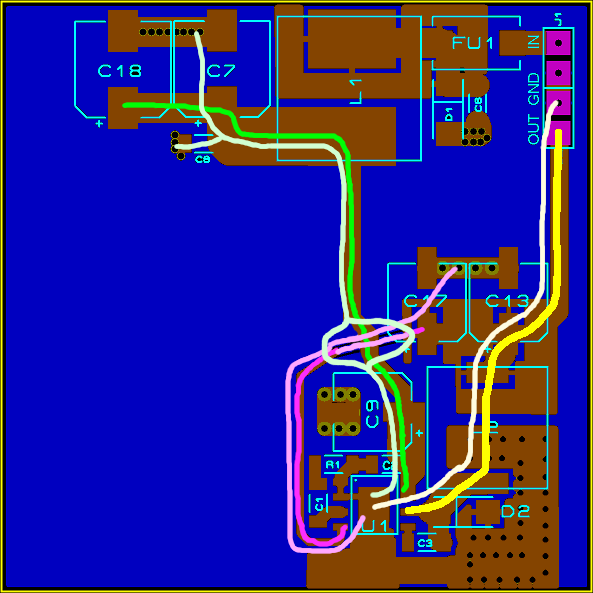
Here is an updated drawing of the current loops for your new layout:

enter image description here

This is much better, the ground returns are separated for clarity but the high frequency content will travel along the ground plane as close to directly under the power traces as it can. I added the feedback path in pink and lighter color denotes current traveling on the ground plane.

A few notes:

  • The paths are still much longer than they need to be. The feedback loop especially is quite long and will travel under the input current. This input is high impedance so any inductive coupling on this trace will have a relatively large impact on your regulation accuracy. You do cross at almost 90 degrees which reduces coupling but the ground currents do not and are an issue for other reasons (see below).

  • The input power trace crosses a split in the ground plane where the trace for the feedback loop runs. Never ever, ever, cross a split on a ground or power plane on an adjacent layer with a trace that has any chance of carrying high frequencies (which means any trace at all really). This creates a radiating loop as indicated by the light green return path. The end result is a large EMI problem.

  • I don't know if it is a result of the export to pdf or what but you seem to have lots of vias that will have clearance issues. They are too close together and too close to the component pads. Even with solder mask over the vias the solder mask clearance on the pads looks like it will expose some of the vias causing soldering issues if you use reflow. The vias near D1 for instance will almost certainly be exposed and when the board is reflowed the via will suck all the solder away from the pad leaving D1 either unsoldered or very poorly soldered.

  • Some vias also don't appear on both layers, such as those under U1.

What I would do:

Setup your PCB design software design rule checking with whatever clearances are required by your PCB fabricator. This will alert you to issues with via-via, via-pad and via-solder mask clearance issues.

Tear the design up and start fresh with component placement knowing that you now have a solid ground plane. Concentrate on minimizing the length of the critical paths and use as much copper as you can for these paths (bar the feedback loop, its low current). If space / layout allows, a ground pour on the surface isn't a bad idea, just make sure you can do it properly. (no orphaned copper, well coupled to the ground plane)

Edit 2:

Not sure if you have this already but here is the reference design / app notes from infineon for a 2 layer board using a solid ground plane on the bottom. They use a fairly long FB trace but keep it well clear of of the dangerous loops.

\$\endgroup\$
5
  • \$\begingroup\$ why did you draw the green starting from whole input? don't C9 and C2 supply the input? how can i solve the poor grounding issue after fulfilling the bottom side of the board with a non separated ground plane? \$\endgroup\$ Commented Aug 12, 2011 at 15:36
  • \$\begingroup\$ The current does go back to the caps, however the only ground path to those cap in your original design was through the trace from C17, then through the Ground pins on the input to get to the ground plane on the other side, then over to the cap grounds through the vias next to those caps. Basically the only path those currents could take to the ground pour on the bottom was through the input connector. \$\endgroup\$
    – Mark
    Commented Aug 12, 2011 at 15:58
  • \$\begingroup\$ @abdullah I updated my answer for your new design with the full ground plane. \$\endgroup\$
    – Mark
    Commented Aug 12, 2011 at 16:38
  • \$\begingroup\$ thanks a lot @Mark, I will re-design it with the things you've cleared out in mind. \$\endgroup\$ Commented Aug 13, 2011 at 10:06
  • \$\begingroup\$ I've re-designed my layout, can you check again? \$\endgroup\$ Commented Aug 15, 2011 at 10:27
6
\$\begingroup\$

There are two high current switching loops in this (and most other SMPS designs) which you need to take care of for sufficient efficiency and low EMI noise.

  1. Pin8 - C9 - GND

    This loop will have to cover your input power.

    To keep the loop itself smaller connect the capacitors ground to the groundflag of you regulator, just rotate C9 90° CCW.

    What I'm missing in your design is some small but fast capacitor, like a 100-220nF ceramic capacitor. Connect it very close to the Regulator IC.

  2. Pin 6 - L2 - C13

    This will be your output loop.

    Move C13 and C17 to the bottom, connect their grounds to the groundtab of the IC (use a nice big polygon fill for that.

    Add a small ceramic capacitor again.

    Rotate L2 180° make a nice large connection (again, a polygon fill would be the best) to C13, C17 and the IC.

    Rotate D2 90° and place it between L2 and the IC., connect it to the polygon and the groundtab.

In general:

  1. Use WIDE traces or polygon fills for all traces with high switching currents.
  2. Use a groundplane if possible, it will reduce noise and will also help conducting heat away from your IC.
\$\endgroup\$
4
  • \$\begingroup\$ Thanks for the info @Masta79, that was the design I was doing before I read AN-1229 from National which says: "In general, the Ground plane should be kept continuous/unbroken as far as possible, or it could behave like a slot antenna. For the switching node therefore, the best option is to keep the amount of copper around it to the actual minimum requirement.". Also, the application note recommends separating AC ground and DC ground where AC ground is noisy switching ground or power ground. Or am I too confused and misleading myself badly? :) \$\endgroup\$ Commented Aug 10, 2011 at 7:21
  • \$\begingroup\$ The best way to "separate" the switching and the system ground in your case is to extend the ground tab of the IC and connect it to system ground at ONE point (usually the cooling vias under the IC). Then connect all the high current ground traces to this ground. Thats basically what I suggested in my answer already ;) Btw, Figure1 on page 2 also shows the current paths. \$\endgroup\$ Commented Aug 10, 2011 at 9:02
  • \$\begingroup\$ So you mean, on the top layer, I should connect signal grounds to the ground tab of the IC -which I should extend for thermal reasons. Then I should connect switching and high current grounds together and then to the system ground in one point which is the ground tab of the IC? And finally, in the bottom layer, I should have a big ground plane that covers the whole board? \$\endgroup\$ Commented Aug 10, 2011 at 9:39
  • \$\begingroup\$ Connect the ground-connection of your input and output capacitors and also your Diode to the ground-tab with a polygon. The biggest problem I currently see with your layout is a bad component placement. The moment you place them in a way that your switching loops are small, your layout will mostly refine itself. \$\endgroup\$ Commented Aug 10, 2011 at 10:17
6
\$\begingroup\$

I would use the adjustable output voltage version of the part rather than the 5v part. But even if the 5v version is used, you should include the feedback voltage divider (just use a zero ohm resistor for the high side, and don't install the low side resistor). This will give you more flexibility in the long run, just in case you need a different voltage.

In general, your traces are not wide enough. Most critical will be the trace from C9 to U1.7-8, anything connected to U1.6, L2 to C17/C13, and GND between U1 and everywhere. These are the nets that will have lots of switching currents and you want to make sure they are short and wide.

U1 could be dissipating some heat, and the connection you have to the GND pad on the bottom of the part isn't going to be enough. You should increase the size of the GND plane on the top side of the PCB. Do this by moving R1 & C1 so the GND plane can expand out from under the chip.

It's hard to tell, but I don't think that you have GND connected between the top and bottom half of the circuit. You really should just have one solid ground plane under the entire PCB and not try to do anything fancy to isolate the different sections. (Exception: you still want the GND plane to cool U1, just use vias to tie that plane to the overall GND plane.)

Conclusion: Thicker traces, better cooling, lots of GND.

Edit: Here's my comments for Rev B...

The bottom should be one complete GND plane. Not split into two halfs. This is critical and should not be ignored.

When possible, don't have GND traces on the top layer-- that's what the GND plane is for. This is especially true for the GND between J1, D1, and C17.

Also, the GND trace to C8 makes that cap completely useless. The trace inductance is going to be huge. Instead use a couple of vias to the GND plane directly at the cap. C8 should probably be located next to C9.

The traces linking the top and bottom half of the circuit are way too thin. Double or triple them. Or better yet, use a copper plane/shape/fill/whatever.

The single trace on the bottom side (from C17 to U1) should be rerouted so that it is mostly on the top of the PCB. This will help keep the GND plane on the bottom more intact and less likely to do bad things.

It's hard to tell from your pictures, but you might need more vias from the GND pad/plane on U1 to the GND plane on the bottom layer. Getting more of the heat to the bottom layer is good.

The GND plane on the top layer that is connected to D2 and goes under L2 needs more vias to the GND plane on the bottom of the PCB. Put at least 2 vias under L2, and maybe a third in the lower right corner.
\$\endgroup\$
5
  • \$\begingroup\$ I cannot understand why I should have a ground plane under entire PCB, shouldn't I isolate grounds of power and signal?By that I don't mean different sections, you are right about that I think. My switching traces aren't big according to AN-1229, as I mentioned in the comment of the other answer. Do you think I misunderstand the application note and exaggerating? Actually the GND is connected with C17.(-) to D1.A, however Proteus somewhat didn't generated that in the bitmap. \$\endgroup\$ Commented Aug 10, 2011 at 7:39
  • \$\begingroup\$ Sorry, by "My switching traces aren't big according to AN-1229", I mean they aren't big because AN-1229 said so :) \$\endgroup\$ Commented Aug 10, 2011 at 8:43
  • \$\begingroup\$ @abdulla kahraman Only in several very specific cases is it advisable to have somewhat isolated ground islands, and this isn't one of them. It is too easy to have variations of GND potential where you don't want one. This could unstabilize the circuit or just increase EMI. You're much better off using a single, huge gnd plane. Make all of the high current nets really wide, and keep all wires as short as possible (especially the switching nodes). AN-1229 is reasonably good, but does not promote the use of isolated ground islands. \$\endgroup\$
    – user3624
    Commented Aug 10, 2011 at 13:48
  • \$\begingroup\$ Absolutely use a solid ground plane, the only connection to ground for your regulator circuit is the trace from C17. This design as it sits would make a very good EMI radiator and the voltage output would be very noisy. In short it would perform terribly and probably not pass FCC part 15 if your current draw is anything significant. \$\endgroup\$
    – Mark
    Commented Aug 11, 2011 at 14:14
  • \$\begingroup\$ @abdulla kahraman I updated my answer to cover your revised PCB layout. \$\endgroup\$
    – user3624
    Commented Aug 11, 2011 at 14:26

Your Answer

By clicking “Post Your Answer”, you agree to our terms of service and acknowledge you have read our privacy policy.

Not the answer you're looking for? Browse other questions tagged or ask your own question.