Alright, one step after the other.
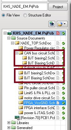
In your CAN Bus Circuit you obviously have two sheet entries (those green rectangles which indicate that a sheet is instantiated here), thereby creating a hierchical project (which is fine). If your sheets are named differently (e.g. BJT Biasing and BJT Biasing2 these should be two separate files). check if you have the correct number of green rectangles.
Also, you should fix alle the errors and warnings from the Compilation process. Press C->R (Compile -> Recompile Project) and you should get a warning dialog (if not, open the messages panel (bottom right, System -> Messages)) and check if it says "Compilation successful, no errors found).). Until you haven't cleared any such warnings in this dialog, there is no use in going further. So: Correct your compilation errors/warnings FIRST.
Assuming you cleared all the compilation issues you are now ready for transferring your design to the PCB. Altium tracks object NOT by their designators BUT by their UniqueIDs. This is most important to understand, if you do not understand this concept, you will not understand where your errors in the transfer process are coming from.
The first time you place an instance of a component on your schematic, it will be assigned a Unique ID (some alpha-numeric value you can see when you double-click the schematic symbol - it is NOT the Designator such as R17, it looks like this: R7AEW3A). Now when the transfer to the PCB is done, this unique ID gets transferred as well (which in turn creates the link between PCB and Schematic).
Now what can happen when you change your Schematic is that you can delete some component and replace it with some other. Let's make an example: U7 is a single Schmitt-Trigger gate in SOT23. We will now replace this with a single inverting Schmitt-Trigger gate in SOT23 (in fact it doesn't even need to be another part, but this should show more clearly what happens). We'll also assume that all parts have already been transferred to the PCB and have been placed at the appropriate places.
So what we do is the following:
- Delete U7 from the Schematic (which removes the Unique ID)
- Add the inverting Schmitt Trigger, name it U7 (now this part has a new unique ID)
- Transfer this to the PCB
Altium will now complain that it has problems with unique IDs ("cannot match components"). Why? Because the U7 footprint on the PCB is linked to the old unique ID, the new U7 yet has a different ID. We will now need to tell Altium that basically the placement for that part is ok and that it's just another part that should be where the old was (which you already placed). Basically you now have two options.
- Remove the footprint from the PCB and then run the design process again (Altium will place the part in the off-board region)
- Use the Project -> Component Links screen. This is the screen which basically matches the two Unique IDs (in fact it removes one and replaces it with the one from the schematic). This is what you should usually do if the change is a minor one as you will keep the placement of the part.
So, now that you understand Unique IDs, back to your problems:
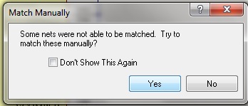
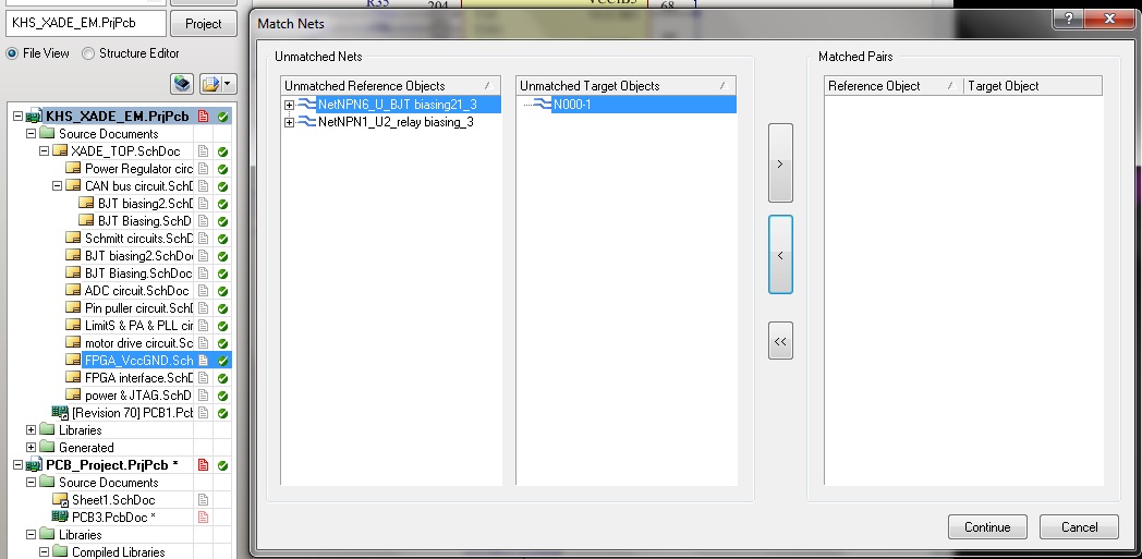
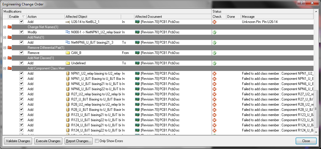
- The "nets" issue isn't a real issue, Altium will remove the nets and add them as it sees fit. Usually after the transfer is done, your nets match up just fine. You can ignore this (I usually do).
- the "Unknown Pin" error is actually bad. This usually indicates that your schematic symbol and footprint doesn't match. Usually you will find that your schematic symbol assigns a net to a pin which doesn't exist in the footprint.
- You can usually ignore the Add Component Class Member warning when doing the validation. You do not show the messages above but probably there is an item where it will add at least one component to the PCB. Unless this is done physically (through the execute Changes command) Altium doesn't detect that the component is actually added and will throw that error message. Run the Execute changes command, Altium will add the footprint(s) and the component class member errors will disappear (of course, make sure that there are NO ITEMS IN THE PROJECT -> COMPONENT LINKS window FIRST).
- Altium removes your differential pair directive (which is bad). Make sure you name your differential pairs CAN_B_N and CAN_B_P and also add the differential pair directive to both of them in the schematic. Personally, I don't see why routing CAN in high speed would be necessary but well ...
Once you sorted out all Project Compilation errors AND Project Links items, the rest should be easy. In case you encounter problems you can't solve, come back here and post them.
One more hint: Is there a specific reason why you would want to copy the sheet physically instead of simply creating a second instance (Hierarchical Multi-Channel Design).


