9
\$\begingroup\$

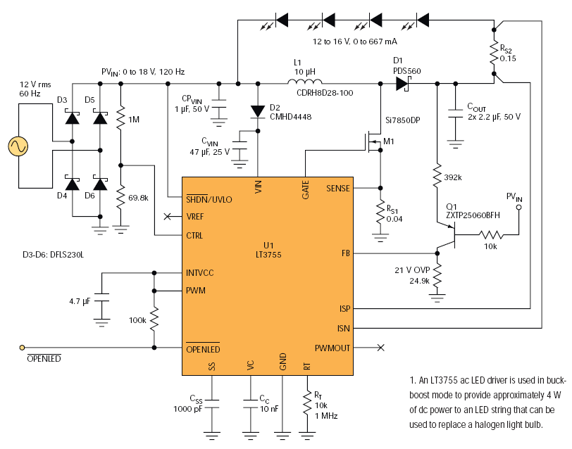
I've been reading up on LED drivers and found some common connection schemes. Yet, I recently came across the following LED driver circuit at this URL:

enter image description here

I tried to find out what exactely was going on here but I do not understand why the LEDs are fed back to the input voltage (usually they are connected to ground). What I understand from the schematic so far:

We have an AC voltage source, this is rectified by diodes D3,D4,D5,D6. CTRL (which sets the current in conjunction to RS2) is set to a fixed level, defined by 1M and 69.8k. SHDN is set to high to enable the device. D2 makes sure that CVIN is constantly charged, thereby keeping VIN enabled (even when there is a zero crossing on the input). OPENLED is pulled up to INTVCC and PWM high enables the device (as well).

Now, the current is driven into L1 (and switched on/off using M1 to achieve a constant current), through D1, through the current sense resistor RS2 (connected to Pins ISP and ISN) and then (and this is the part I really don't get) back to PVIN.

So, actually there's three parts I do not understand:

  • Why is the string of LEDs not terminated at ground (I have seen this multiple times with other LED drivers and also the application note for this LED driver has a similar connection scheme). What would the voltage before the first LED be (since there is a voltage drop across the 4 LEDs)

  • What exactely is the purpose of the FB. The datasheet mentions "Voltage Loop Feedback Pin". But I do not understand the use of the transistor and the 392k resistor.

  • What is the use of RS1 (being 40mR)

It would be really nice if you could shed some light on this specific configuration.

This is the link to the datasheet of the LT3755.

\$\endgroup\$

1 Answer 1

11
\$\begingroup\$
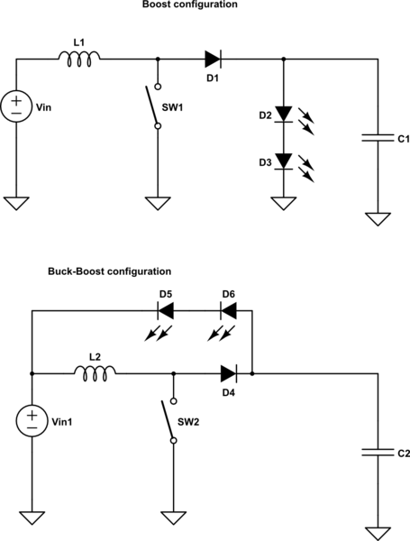
  1. It's a buck-boost configuration. If it was connected in boost then the input voltage could not exceed the LED voltage or they would burn out. There's more voltage across the inductor and the switch has to withstand more voltage with buck-boost.

schematic

simulate this circuit – Schematic created using CircuitLab

  1. The voltage feedback is to protect the IC if the LED string should become open circuit for some reason, otherwise the voltage at Cout would quickly rise to destructive levels. The transistor effectively level shifts the overvoltage protection so that it measures the voltage above the positive rail (more than about 20V plus one Vbe above PVin will cause 50uA to flow, which will drop 1.25V across the 24.9K resistor, which in turn will cause it to shut down).

  2. RS2 is the sense resistor for measuring the LED current. RS1 is the sense resistor for measuring the inductor current.

\$\endgroup\$
2
  • \$\begingroup\$ Your circuit diagram for the buck-boost circuit is missing a capacitor. This is not a nitpick, it's relevant to the operation of the circuit with the LED string folded back to the inductor. The return path for the LED current is through L2 and M1, because on the previous cycle the converter boosted a little more energy onto Cout. A very clever circuit, as it doesn't require a separate inductors and switches for the boost and buck stages. \$\endgroup\$
    – dbrwn
    Commented Aug 9, 2015 at 15:42
  • 2
    \$\begingroup\$ @DaveB okay, added the output caps. I didn't want to obscure the switch-inductor-load configuration too much by adding on too much stuff. You can think of it as a complementary form of the usual single-inductor inverting buck-boost, with the same issues. \$\endgroup\$ Commented Aug 9, 2015 at 15:54

Your Answer

By clicking “Post Your Answer”, you agree to our terms of service and acknowledge you have read our privacy policy.

Not the answer you're looking for? Browse other questions tagged or ask your own question.