0
\$\begingroup\$

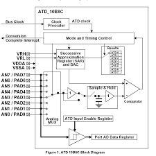
For a Hcs129s12 micro-controller ADC (please see the image) , the sample-and-hold stage accepts analog signals from the input multiplexer and stores them as a charge on the sample capacitor. The sampling process has two stages: 1. Initially, a sample amplifier (of unity gain) is used to buffer the input analog signal for two cycles to charge the sample capacitor almost to the input potential. This stage reduces charging and discharging the sample capacitor by the signal source. 2. The sample buffer is then disconnected and the input signal is directly connected to the storage node for programmable 2, 4, 8, or 16 cycles. The conversion time of a sample is given by the following equation:

Conversion time =(no. of bits in resolution + no. of programmed sample clocks + 2)/ ATD clock frequency

enter image description here

I have a question about step 2: when the sample buffer is disconnected and the input signal is directly connected to the storage node for programmable 2, 4, 8, or 16 cycles, does it mean that we store the voltages during the time that the sample buffer is disconnected? If so why we assign a register to this task if we never use this data?

\$\endgroup\$
1
  • \$\begingroup\$ Reference: THE HSC129S12: an introduction to software and hardware interfacing \$\endgroup\$
    – Jack
    Commented Oct 6, 2015 at 17:10

2 Answers 2

2
\$\begingroup\$

No. What it means is that in Step 1, the hold capacitor is charged to nearly the right voltage by the unity gain amplifier just to the left of the Sample&Hold (S&H) block. But that amplifier is not particularly accurate.

So then in Step 2 the switch between amp and S&H connects the capacitor directly to the selected input channel, to charge the capacitor exactly to the input voltage. How long that takes is a function of the source impedance of the signal. As that source impedance is external to the chip, it is unknown to the chip designers how long this takes. So the device caters for higher source impedances by allowing that final charging time to be programmable. You select the sample buffer time according to the external circuitry.

AFTER this step, the S&H is switched into "Hold" mode which means the input voltage is now stored on that capacitor - not a register - for the next 10 cycles (for a 10 bit conversion) while the conversion takes place.

\$\endgroup\$
7
  • \$\begingroup\$ I can not see how the capacitor is getting connected directly to the input voltage in the image. Could you please elaborate more. \$\endgroup\$
    – Jack
    Commented Oct 6, 2015 at 17:30
  • \$\begingroup\$ See the wire that bypasses the amplifier? Via that. \$\endgroup\$
    – user16324
    Commented Oct 6, 2015 at 17:31
  • \$\begingroup\$ Yes I see it, thank you. So what is the other amplifier does( the one at the bottom) that is connected to port AD register? I thought that this where we store the voltage when the input buffer is disconnected. \$\endgroup\$
    – Jack
    Commented Oct 6, 2015 at 17:33
  • \$\begingroup\$ See the squaring symbol inside it? (Schmitt trigger) The databook should tell you for sure, but I'm pretty sure that treats all 8 inputs as digital inputs, not analog. The "ATD Input Enable Register" selects some or all of those bits as digital inputs (according to teh value you program into it) and the "Port AD Data Register" reads the selected digital inputs. Nothing to do with storing voltage. \$\endgroup\$
    – user16324
    Commented Oct 6, 2015 at 18:05
  • 2
    \$\begingroup\$ It's an alternative way of using the pins. If you need to read 2 analog voltages and 6 switches for example, you might use pins AN0 and AN1 for the analog signals, with switches connected to pins AN2/PAD2 to AN7/PAD7. Then tell the CPU which is which (by writing "ATD Input Enable Register") and read the switches by reading "Port AD Data Register". You only need to do a conversion for an analog signal (e.g. on AN0 or AN1). \$\endgroup\$
    – user16324
    Commented Oct 6, 2015 at 18:12
1
\$\begingroup\$

This is a clever way to allow for faster ADC sampling rates, especially for sources with high output inpedances.

As the output impedance of an analog source increases, so too increases the amount of time it takes to charge (or discharge) the sampling capacitor. This is an upward limit on possible sampling speed.

This microcontroller gets around the problem by using the unity-gain buffer to provide ample current to the sampling capacitor. It quickly "gets close" to the input voltage. Then, in the next step, the actual source is connected to the same sampling capacitor. At this point there is only a small voltage differential, and so little current needs to flow from the analog source.

\$\endgroup\$
2
  • \$\begingroup\$ So when the fast ADC is not needed, then we can simply connect it without the unity gain buffer? \$\endgroup\$
    – Jack
    Commented Oct 6, 2015 at 18:04
  • 1
    \$\begingroup\$ @MaryE From an electrical standpoint, yes, certainly. In fact, other microcontrollers I have used (PIC18, STM32F1) use only direct connections. Practically speaking, however, your specific micro may not have an option to not use the buffer... \$\endgroup\$
    – bitsmack
    Commented Oct 6, 2015 at 18:27

Your Answer

By clicking “Post Your Answer”, you agree to our terms of service and acknowledge you have read our privacy policy.

Not the answer you're looking for? Browse other questions tagged or ask your own question.