2
\$\begingroup\$

I'm looking for a digital circuit whose behavior I will describe in a moment. It has one digital input (5V logic) and two digital outputs (12V logic). I'll hereby refer to these levels as 0 and 1, but keeping in mind the voltage difference between input and output. This circuit has to be as cheap as possible, with simplicity the second priority.

Upon a rising edge on the input, the first output should immediately go to 0, while the value of the second output is irrelevant (don't care).

Upon a falling edge on the input, both outputs should immediately go to 1. After an interval of time (around 200 ms, up to 50% tolerance on the timing is still acceptable), the second output should go to 0.

I built a circuit for this that would work if the input was 12 V, but other considerations forced the voltage level on the input to 5 V. I already felt my solution was getting complicated for a 12 V input, and just piling on a level shifter from 5 to 12 V would further complicate this circuit, so I'm trying to start from scratch and think of a simpler solution.

I think posting my circuit here would be counterproductive, as the natural reaction would be trying to refine it, and I think a good solution demands some outside the box thinking, but I will edit the post to include the circuit if requested by anyone.

Edit: by request, here is the circuit:
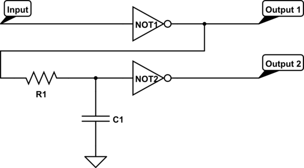
schematic

simulate this circuit – Schematic created using CircuitLab

The NOT gates are Schmitt triggers (HCF40106 in my circuit), which is why the circuit doesn't work properly with a 5V input: 5V is not recognized as a high level signal when the Schmitt triggers are supplied with 12V.

To fix the 5V issue, I thought of passing the input through the following circuit, but as stated above, I believe this is getting more complicated than necessary:
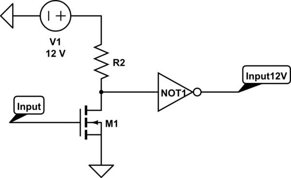
schematic

simulate this circuit

\$\endgroup\$
4
  • \$\begingroup\$ Is using a single NPN transistor on the input too complicated? \$\endgroup\$
    – Nedd
    Commented Nov 22, 2015 at 3:01
  • \$\begingroup\$ Alternately, the input and all the middle logic could use 5V, then use an NPN transistor on each output to switch the required 12V signal. \$\endgroup\$
    – Nedd
    Commented Nov 22, 2015 at 3:13
  • \$\begingroup\$ Also, the possibility of using one small dual op-amp chip instead of logic devices. The op-amp uses a 12V supply, the first op-amp switches with a 5V input and provides 12V (hi-lo) to the first output, the second op-amp provides the delay for the second output. \$\endgroup\$
    – Nedd
    Commented Nov 22, 2015 at 3:23
  • \$\begingroup\$ Please post your circuit. \$\endgroup\$
    – EM Fields
    Commented Nov 22, 2015 at 12:38

4 Answers 4

2
\$\begingroup\$

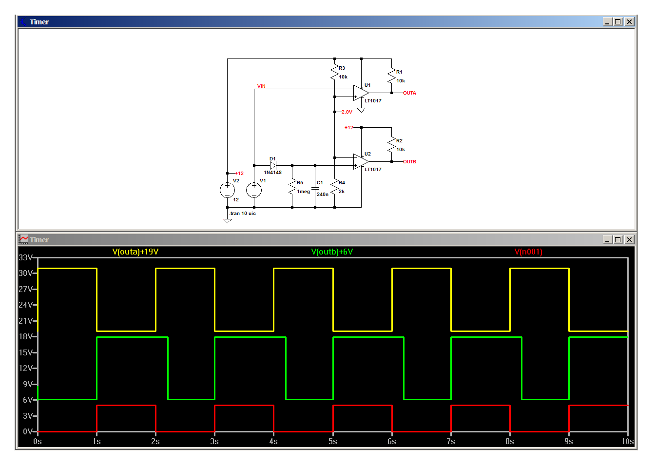
I've shown an LT1017 for convenience, but a cheap LM393 would work just as well, as would a cheap opamp, in which case you could eliminate the 10k pullups.

Also, both outputs swing between 12 volts and ground, but I've manipulated the plot for clarity.

The LTspice circuit list follows, just in case you want to play with the circuit.

enter image description here

Version 4
SHEET 1 880 680
WIRE 112 -16 -336 -16
WIRE 224 -16 112 -16
WIRE 352 -16 224 -16
WIRE 112 0 112 -16
WIRE 352 16 352 -16
WIRE 224 96 224 -16
WIRE -192 112 -224 112
WIRE 192 112 -192 112
WIRE 352 128 352 96
WIRE 352 128 256 128
WIRE 400 128 352 128
WIRE 112 144 112 80
WIRE 192 144 112 144
WIRE 224 192 224 160
WIRE 112 208 112 144
WIRE 144 208 112 208
WIRE 224 272 192 272
WIRE 352 272 224 272
WIRE 352 304 352 272
WIRE 224 384 224 272
WIRE 112 400 112 208
WIRE 192 400 112 400
WIRE 352 416 352 384
WIRE 352 416 256 416
WIRE 400 416 352 416
WIRE -224 432 -224 112
WIRE -176 432 -224 432
WIRE -64 432 -112 432
WIRE 32 432 -64 432
WIRE 192 432 32 432
WIRE -336 464 -336 -16
WIRE -304 464 -336 464
WIRE -64 480 -64 432
WIRE 112 480 112 400
WIRE -336 496 -336 464
WIRE -224 496 -224 432
WIRE 32 496 32 432
WIRE -336 608 -336 576
WIRE -224 608 -224 576
WIRE -224 608 -336 608
WIRE -64 608 -64 560
WIRE -64 608 -224 608
WIRE 32 608 32 560
WIRE 32 608 -64 608
WIRE 112 608 112 560
WIRE 112 608 32 608
WIRE 224 608 224 448
WIRE 224 608 112 608
WIRE -336 656 -336 608
FLAG 400 128 OUTA
FLAG 400 416 OUTB
FLAG 224 192 0
FLAG 144 208 2.0V
FLAG -336 656 0
FLAG 192 272 +12
FLAG -304 464 +12
FLAG -192 112 VIN
SYMBOL Comparators\\LT1017 224 128 R0
SYMATTR InstName U1
SYMBOL Comparators\\LT1017 224 416 R0
SYMATTR InstName U2
SYMBOL res 336 0 R0
SYMATTR InstName R1
SYMATTR Value 10k
SYMBOL res 336 288 R0
SYMATTR InstName R2
SYMATTR Value 10k
SYMBOL res 96 -16 R0
SYMATTR InstName R3
SYMATTR Value 10k
SYMBOL res 96 464 R0
SYMATTR InstName R4
SYMATTR Value 2k
SYMBOL diode -176 416 M90
WINDOW 0 0 32 VBottom 2
WINDOW 3 32 32 VTop 2
SYMATTR InstName D1
SYMATTR Value 1N4148
SYMBOL res -80 464 R0
SYMATTR InstName R5
SYMATTR Value 1meg
SYMBOL cap 16 496 R0
SYMATTR InstName C1
SYMATTR Value 240n
SYMBOL voltage -224 480 R0
WINDOW 3 24 96 Invisible 2
WINDOW 123 0 0 Left 2
WINDOW 39 0 0 Left 2
SYMATTR InstName V1
SYMATTR Value PULSE(0 5 0 1u 1u 1 2)
SYMBOL voltage -336 480 R0
WINDOW 123 0 0 Left 2
WINDOW 39 0 0 Left 2
SYMATTR InstName V2
SYMATTR Value 12
TEXT -328 632 Left 2 !.tran 10 uic
\$\endgroup\$
1
  • \$\begingroup\$ Although I initially marked another answer as the accepted answer, I now realize yours is essentially the same, and the diode is a nice finishing touch. Hence I changed the accepted answer to yours. Thanks! \$\endgroup\$
    – swineone
    Commented Nov 22, 2015 at 18:37
1
\$\begingroup\$

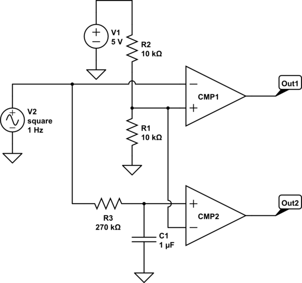
Would the following circuit, using comparators, work?

schematic

simulate this circuit – Schematic created using CircuitLab

Here are some simulation plots (input on the first one, outputs on the second one):

Simulation plot

Simulation plot

The only issue is that when the input is pulsed twice in a short time (less than 1 second or so), the capacitor will be caught up halfway through charging or discharging, which will affect the pulse timing. Since you don't need absolute precision this may be acceptable.

\$\endgroup\$
1
  • \$\begingroup\$ Perfect, this is exactly what I was looking for! \$\endgroup\$
    – swineone
    Commented Nov 22, 2015 at 18:26
0
\$\begingroup\$

the common 555 timer chip can have the input voltage levels tweaked by means of the control voltage pin, so put 3V or so on the control voltage pin to get it compatible with 5V CMOS signals and wire one 555 as an inverter and the other as a monostable.

\$\endgroup\$
1
  • \$\begingroup\$ I wpuld drow a schamatic but curcuitlab does not even have a vaguley realiastic 555 model \$\endgroup\$ Commented Nov 22, 2015 at 3:46
0
\$\begingroup\$

Your logic is crying out for a microcontroller. Fortunately, micros with 2 inputs and 2 outputs that can perform the logic you describe are cheap and small. Even the tiny PIC 10F200 can do this. No kludgy and bulky analog electronics are required, just the PIC and its bypass cap. It has a internal oscillator good to a few percent, which is well within your accuracy spec, and better than external resistors and caps on a 666 555 timer and the like would give you.

You will need something to convert the 5 V output from the micro to the 12 V you need. This could be as simple as a single "logic level" FET for each signal, like the IRLML2502. That would actively drive low and require a passive pullup. I'll leave it at that since you haven't specified what the source/sink capabilities and speed of the outputs need to be.

\$\endgroup\$

Your Answer

By clicking “Post Your Answer”, you agree to our terms of service and acknowledge you have read our privacy policy.

Not the answer you're looking for? Browse other questions tagged or ask your own question.