1
\$\begingroup\$

This is a 2 part question for my understand about how an MOSFET/IGBT based active rectifier controls current.

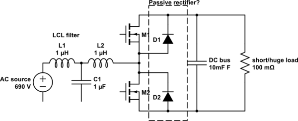
1) Assuming a 3 phase active front end to a DC bus, and some huge load on the DC bus attempted drawn below. (Only 1 phase drawn, ignore exact values)

schematic

simulate this circuit – Schematic created using CircuitLab

Once the short/big load makes the DC bus voltage drop, won`t this effectively become a passive rectifier through its diodes? Which in turn would give it no way of blocking its current?

2) In normal operation I assume its diodes also works as passive rectifiers. With its transistors are only used for boosting input voltage...?

\$\endgroup\$

2 Answers 2

4
\$\begingroup\$

You are correct, the active rectifier has no way of blocking current. A safety device needs to be provided separately to protect against short circuit. Passive rectifiers have the same problem.

The MOSFETs are there not to boost voltage but to get better efficiency. MOSFETs can have a very low on resistance sometimes as low as tens of miliohms. An average diode has a forward operating voltage 0.6v to 0.7v and if passing 10A the power dissipation is 6W. If the MOSFET has a RDSon of 20mOhm then the power dissapated is 2W.

\$\endgroup\$
3
  • \$\begingroup\$ But can an N channel MOSFET conduct in that direction even while on? (source=>drain) \$\endgroup\$
    – Imbrondir
    Commented Dec 19, 2015 at 15:17
  • 2
    \$\begingroup\$ @Imbrondir The channel that forms in a MOSFET is bidirectional but normally not characterized source to drain because of the body diode. \$\endgroup\$
    – vini_i
    Commented Dec 19, 2015 at 15:31
  • 3
    \$\begingroup\$ At high currents practical Si diodes have a drop of around 1V which is far away from the .6 that is taught in colleges.The on resistance of the mosfet in this reverse mode is about 20% lower than the datasheet foward value .These facts make the active rectifier less unattractive.However as temp rise RDs on goes up and diode drop goes down. \$\endgroup\$
    – Autistic
    Commented Dec 19, 2015 at 21:41
0
\$\begingroup\$

Adding my own answer after I`ve learned a lot more about usage of passive rectifiers:

2) In normal operation I assume its diodes also works as passive rectifiers. With its transistors are only used for boosting input voltage...?

Yes. Transistors are present mainly for boosting DC voltage. This gives several benefits.

Partial load control

If there is a malfunction on the rectifier side (high temperature, low frequency..etc) it could stop boosting, which in turn drops DC voltage. If consumers of the DC link are all inverters, they can have an undervoltage limit, and stop consuming.

After of which the system might recover, and rectification can continue. If not, supply can be broken without current, which is much easier on the breaker.

As vini_i mentioned this will not help if the DC link itself is shorted.

Current control

Increasing DC link above rectifier levels means the booster controls when the current should be drawn. This means current spikes when AC voltage peaks can be completely avoided, and draw pure sine waves of current. This means less transients and THD on the supply network.

Power factor compensation

If you can control when to draw current, you can also control the phase of the current compared to supply voltage. This in turn means you can have almost any desired power factor. Which generally means lower overall current, less I^2*R copper losses, and in turn higher efficiency.

Quote: vini_i: The MOSFETs are there not to boost voltage but to get better efficiency

The part about efficiency is still true. If the transistors are MOSFETs they could be used as a more efficient diode. Generally called a synchronous rectifier.

This is NOT the case for IGBTs however, since they can only conduct in one direction. They are also usually the transistor of choice in 690V applications as mentioned in the original question.
\$\endgroup\$
2
  • \$\begingroup\$ This doesn't make sense: "Transistors are present mainly for boosting DC voltage". \$\endgroup\$
    – Navin
    Commented Feb 6, 2020 at 8:44
  • \$\begingroup\$ @Navin . It does make sense. When the input voltage is positive, the bridge forms a boost converter. Charging the input inductor with low side FET, then high side becomes the boost diode, or synchronous diode. Then the opposite arrangement when input voltage is negative. This way you can pull current almost whenever you want, instead of only during voltage peaks. \$\endgroup\$
    – Imbrondir
    Commented Feb 6, 2020 at 11:15

Your Answer

By clicking “Post Your Answer”, you agree to our terms of service and acknowledge you have read our privacy policy.

Not the answer you're looking for? Browse other questions tagged or ask your own question.