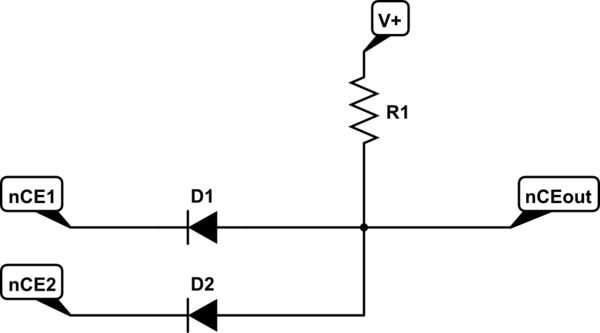
My VIC-20 has a few bank select lines that are used for enabling ROM chips on the cartridge port. When one of them goes low, it means that a certain 8KB region of the address space has been accessed.
Usually you can hook these up directly to the chip enable (/CE) pin of a ROM chip to essentially place that 8KB ROM into a certain slot in memory.
However, I have a 16KB ROM with only one /CE pin which means that I need to combine two bank select lines. I know I can do this with a single AND gate (since the logic is inverted), but it seems like a waste to use a quad-AND or NAND chip if there was a simpler solution.
Note, only one of the bank select lines ever goes low at a time. So the truth table would be kind of like:
A|B|O
-----
1|1|1
0|1|0
1|0|0
0|0|Never happens
Is there an elegant way to do this with discrete components?

