3
\$\begingroup\$

In preparation to design my own boost converter, I am trying to analyze the poorly-performing 555 boost converter circuit discussed here (so that I know which mistakes to avoid):

555 timer boost converter doesn't meet spec

The circuit is reproduced here for convenience: 555 boost converter
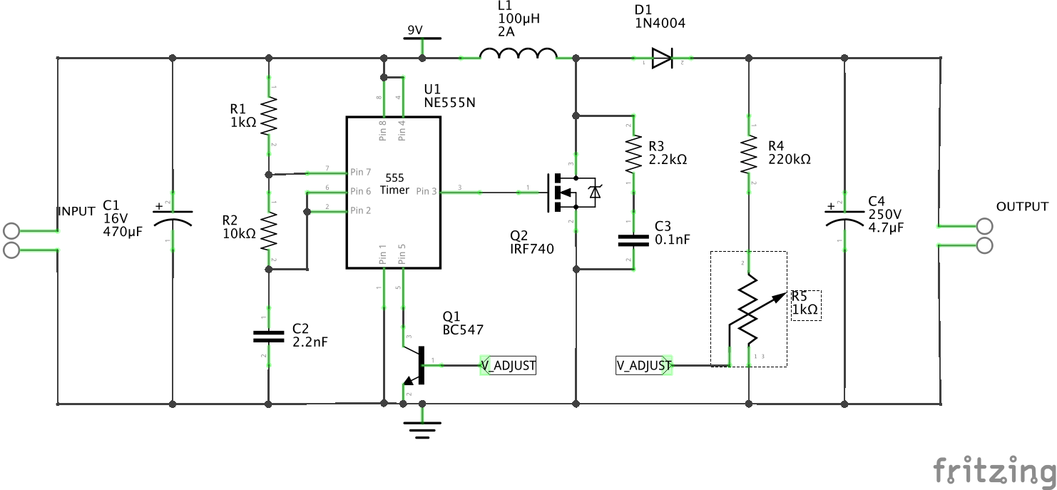
The accepted answer's comments suggested that the power MOSFET attached to the 555 has a switching-on time in the microseconds range and a current of approximately 1 mA. While I trust the posters' judgments, they do not explain how they reached those values. I wanted to try to calculate the expected switching time on my own and see if I could reproduce the results.

Using an IRF740 datasheet and an appnote (not enough rep to post the links) for calculating the switching speed during turn-on, I found the following equation: $$ t_{ir} = (R_g + R_{g\_app})*(C_{iss}~at~V_{DS})*\ln(\frac{g_{fs}(V_{GS\_APP}-V_{th})}{g_{fs}(V_{GS\_APP}-V_{th})-I_{DS}}) $$

where:

  • \$R_g\$ is gate resistance.
  • \$R_{g\_app}\$ is external gate resistance (0 Ohms).
  • \$C_{iss}\$ is input capacitance (1400pF @ 9V).
  • \$I_{DS}\$ is Drain-Source current.
  • \$g_{fs}\$ is forward transconductance (5.8 S).
  • \$V_{Th}\$ is threshold voltage (4V worst case).

I made the following assumptions when trying to calculate switching time with the above equation:

  • \$R_g\$ is not given. Assume 1 Ohm.
  • Input \$V_{GS}\$ is 9 - 1.7 = 7.3 Volts, according to voltage drop from 555.
  • \$I_{DS}\$ at maximum is 1.44 Amps (worst case), according to the linked answer.
  • Inductor current is constant just before switch, so MOSFET sees 9V across drain and source.
  • \$C_{iss}\$ is assumed from chart (25C) on page 3 of the datasheet.

When I do the calculation, my predicted switching speed is approximately: $$ 1.4*10^{-9}*\ln(\frac{5.8(3.3)}{5.8(3.3)-1.44}) = 1.09*10^{-10}s $$

My calculated switching time seems orders of magnitudes too fast, considering the output current calculated is in the milliamp range. Does anyone have an idea of what assumptions I made that do not hold, and what assumptions I should replace? It would be nice if I can get my predicted current and switching speed within an order of magnitude of previous analyses done by others (which I assume to be correct).

\$\endgroup\$
5
  • \$\begingroup\$ IRF740 datasheet: vishay.com/docs/91054/91054.pdf MOSFET switching time APNOTE: vishay.com/docs/73217/73217.pdf \$\endgroup\$
    – cr1901
    Commented Dec 30, 2015 at 6:14
  • \$\begingroup\$ I don't see where the accepted answer to the linked question "suggested that the power MOSFET attached to the 555 has a switching-on time in the microseconds range and a current of approximately 1 mA." What it does say is "The MOSFET has a total gate charge of 63 nC, and the 555 has a maximum output current of about 200 mA, which means it takes a minimum of 63 nC / 200 mA = 315 ns to charge or discharge the gate.", which is pretty straightforward, and also shows the calculation used to determine the switching time. \$\endgroup\$
    – The Photon
    Commented Dec 30, 2015 at 6:26
  • \$\begingroup\$ Oh dear... that was my comment, wasn't it... \$\endgroup\$
    – W5VO
    Commented Dec 30, 2015 at 7:12
  • \$\begingroup\$ The 555 circuit is on the internet .... it must be good ?! \$\endgroup\$
    – Autistic
    Commented Dec 30, 2015 at 7:36
  • \$\begingroup\$ @Autistic The idea was to analyze what made this circuit so poor (such as long switching times) and see if I could correct the circuit; I'm now realizing that 555 is the wrong IC for the job period. Goal is to design a simple, purely analog boost converter (PWM control IC, not microcontroller w/ ADC). \$\endgroup\$
    – cr1901
    Commented Dec 30, 2015 at 12:17

1 Answer 1

2
\$\begingroup\$

Well, the guy that wrote that comment is an idiot. What should have been more clearly expressed was that at a switching frequency of 30 kHz, the energy spent to just switch the MOSFET is probably about 1 mA (out of the 100 mA you are measuring on the input). This was in response to the original version of the answer saying that all 100 mA was being used to switch the MOSFET gate. This is different from the peak magnitude of the gate drive current, which is heavily dependent on your 555 output.

So on to the 1-2 µs switching time figure... that was a guess because there were no oscilloscope waveforms. It is incredibly difficult to troubleshoot some circuits (or some "failure" modes) without any oscilloscope over the internet. I still think poor switching time is a reasonable guess (and maybe 1-2 µs is a bit high, but it's an estimate that's within an order of magnitude). Note that you can effectively prolong your switching time beyond the design spec if the MOSFET oscillates during switching.

Current saturation of the inductor is also a reasonable guess, and some proper ripple current analysis for a boost converter would really answer whether the inductor is appropriately sized.

@Autistic points out that the diode, as specified, is a 1N4004, which is a terrible choice for a switch mode converter. Slow diodes don't turn off quickly, which means that the output is discharging through the diode into the power MOSFET. Obviously, this is bad, so pay attention to the reverse recovery time of a diode when you're picking one out.

The system may also be unstable in a no-load configuration, as you will need to have a discontinous current mode operation in order to maintain the voltage. These are things that can go wrong, and without sufficient information all we can do is throw stuff at the wall and see what sticks. I think we were looking for 90mA of input waste or so.


On to your equations:

First off, be honest with your numbers (or worry when you start setting important variables to zero). You may not have a resistor in series between the 555 output and the MOSFET gate, but that doesn't mean that the external drive resistance is 0Ω. The Photon points out that the current rating for a 555 output is 200 mA, which gives an optimistic 45Ω. The internal gate resistance seems reasonable.

The next thing to mention is that the equation you mention (which is equation 17 in the linked app note) is only the switching time for the drain current! Note that equation 18 covers the voltage switching, and that time gets added to your current switching time. Understand that this is for a configuration commonly called a "clamped inductive load", meaning an inductor with a diode return path. Look at Fig. 4-6 in that app note and make sure you understand what is happening and why - it is not intuitive for many people.

Now with hopefully most misconceptions removed, lets look at the actual switching time from equations 17 and 18, with numbers. I'll use your numbers, with the following exceptions:

  • Rg_app = 45Ω (probably low, but lets go with it)
  • Qgd_d = 21nC (estimated from Fig. 6 in the MOSFET datasheet, 200V curve)
  • Vf_d = 0V (Vds_off >> Vf_d)
  • Vf = 0V (Vds_off >> Vds_on)
  • Vds_off = 170V (assuming steady-state condition), Ciss = 1.25nF

\$t_{ir}=(R_g+R_{gext})C_{iss} \ln(\dfrac{g_{fs}(V_{GSAPP}-V_{th})}{g_{fs}(V_{GSAPP}-V_{th})-I_{DS}}) = 4.5ns\$ \$t_{vf}= \dfrac{Q_{gdd}V_{DS}(R_g+R_{gext})}{V_{DS}(V_{GSAPP}-\dfrac{I_{DS}}{g_{fs}})} = 134ns \$

This gives a total turn-on time of about 140ns, if our assumptions are valid and everything is going right. Note that even in the app note, the calculated tvf was 1/3 the measured tvf. Read what the app note says about their calculations. Also, read through the wikipedia article on boost converters, that will help understanding the system. And finally, don't use a 555. There are hundreds of better alternatives for what you want to do that are not hacks that will work better.

\$\endgroup\$
6
  • 1
    \$\begingroup\$ The guy that specified a slow 1N4004 is an Idiot.The slow diode will make the FET run hot.In fact the fet will waste more than the slow diode.Sort out the diode and consider millar killer and then the equations wont be so optimistic. \$\endgroup\$
    – Autistic
    Commented Dec 30, 2015 at 9:54
  • 1
    \$\begingroup\$ "Well, the guy that wrote that comment is an idiot." lol...nice \$\endgroup\$
    – efox29
    Commented Dec 30, 2015 at 11:40
  • \$\begingroup\$ @W5VO Thank you for the clarification/corrections- accepting! I won't use a 555; I'll look for a better analog IC (the idea is to do a purely analog boost converter for fun). Just one question: Should I treat the 1mA that you mentioned as an average current, since the gate drive current will vary (per the RC filter behavior of the gate source) as gate charge is added? \$\endgroup\$
    – cr1901
    Commented Dec 30, 2015 at 12:19
  • \$\begingroup\$ @Autistic Oh yes, a 60Hz rectifying diode will also be a terrible drain on efficiency. I'm unfamiliar with the term "Miller Killer". A brief search identified some Unitrode (now TI) documentation that made it look like "just" a high current gate driver - am I missing something? I'll definitely agree that a high current driver would help. \$\endgroup\$
    – W5VO
    Commented Dec 30, 2015 at 15:48
  • \$\begingroup\$ @cr1901 The 1-2mA current is purely average current, based on the fact that when you charge the gate capacitance, you inject 63nC. Doing this 30,000 times per second adds up: I=q/t, and frequency is 1/t, so I = q*f = 63nC * 30kHz = 1.89 mA. If you use a high current gate driver, your peak current can be in the 4-8A range during switching, and 0 during steady state. \$\endgroup\$
    – W5VO
    Commented Dec 30, 2015 at 15:56

Your Answer

By clicking “Post Your Answer”, you agree to our terms of service and acknowledge you have read our privacy policy.

Not the answer you're looking for? Browse other questions tagged or ask your own question.