6
\$\begingroup\$

I am building a battery-powered uC circuit with an RGB LED. The LED is common cathode, so the circuit for switching the LED elements has to be high-side. The LED is a higher-current LED, so it cannot be driven by the uC directly.

To save power, I was planning to have the uC (AVR ATmega328) run at whatever voltage the 2 AAA batteries will provide (1.8-3.0V), while the LEDs need to be driven at 4.0V to account for the LED vdrop - the plan was to use a boost converter to power the LEDs. I was wondering what is the best way to drive the LED output from the uC. I can think of a few ways:

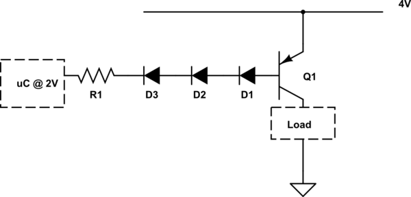
PNP BJT switch with three diodes

AVR docs state that the chip cannot "see" more then 0.5V above Vcc on any of the pins, so one option would be to use a diode \$V_{forward}\$ to present a lower voltage to the uC:
schematic

Perhaps D1 can be omitted? I am not sure if there is a E->B voltage drop in a PNP transistor.

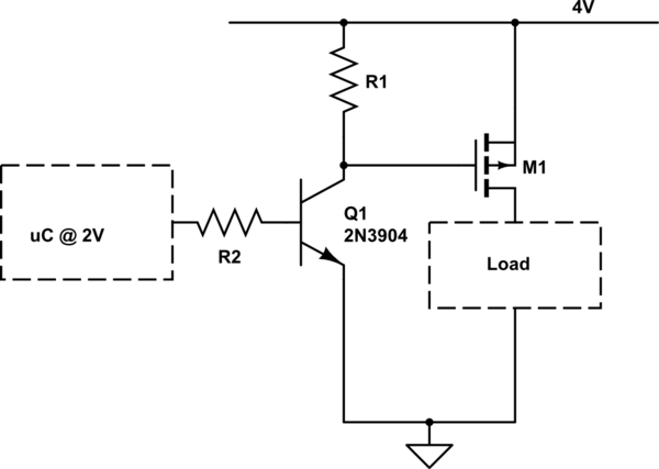
P-Channel MOSFET with an NPN BJT

Another option is to control the P-Channel MOSFET with an NPN BJT
schematic

simulate this circuit – Schematic created using CircuitLab

N-Channel high-side MOSFET switch

This requires a charge-pump or something equivalent, so I am leaning against this solution.


Currently I am leaning towards the second solution, for no particular reason. Are there other solutions I should be considering? Are there other considerations that I should be thinking about?

\$\endgroup\$
6
  • 2
    \$\begingroup\$ P-Channel MOSFET with an NPN BJT is the simplest choice. No real component-matching is required; you can build it with whatever you have lying around. If Q1 were a MOSFET (with low Vgs threshold) you could do away with R2. \$\endgroup\$ Commented Jan 1, 2016 at 18:17
  • 2
    \$\begingroup\$ I agree with @CharlieHanson. Just want to add that the diodes will not really protect the uC input against high voltage, because the diode voltage will be zero unless some small current flows. Also wanted to add that a PNP BJT does have one diode drop between emitter and base. \$\endgroup\$
    – user57037
    Commented Jan 1, 2016 at 18:46
  • \$\begingroup\$ Ah, good point about R2 @CharlieHanson - hice. \$\endgroup\$ Commented Jan 1, 2016 at 18:49
  • 1
    \$\begingroup\$ +1 and a favorite question. Nicely done, and a pleasure to read. Clearly written, with the problems described verbally and tentative solutions presented as schematics instead of words. \$\endgroup\$
    – EM Fields
    Commented Jan 1, 2016 at 18:52
  • \$\begingroup\$ related: electronics.stackexchange.com/a/106673 \$\endgroup\$ Commented Jan 2, 2016 at 0:44

2 Answers 2

3
\$\begingroup\$

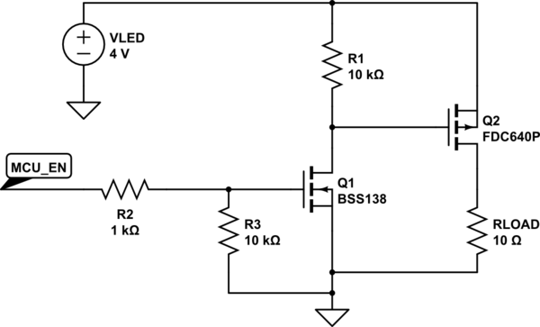
Yeah, I think Option 2 is your simplest high-side option. Replace Q1 with a BSS138, and you can have a simple all MOSFET solution with discrete parts.

Alternately, if you're OK buying ICs, you can use an IC like the TPS2557 (which is an N-channel load switch with built-in charge pump), or an integrated dual N/P part like the Si3865DDV which basically squeezes the option 2 circuit into a convenient package. These would also take up less space than the discrete solution, and offer some protection features such as current-limiting if you would like. I can also understand the appeal of building something with parts you have lying around.

A N-channel device will have a lower on-resistance than a comparable P-channel device, but it does require a charge pump as you stated.

Finally, even with a MOSFET solution, I would personally keep R2 there and make it 1k or so, in addition to adding a pull-down to your UC enable pin so that when you are in reset, the LEDs stay off. By keeping R2, if you drop a screwdriver or something across the gate of the MOSFET to GND, it limits the current that can flow from the uC pin.

Here's the discrete solution:

schematic

simulate this circuit – Schematic created using CircuitLab

\$\endgroup\$
1
\$\begingroup\$

I vote for the second solution because the first one's kind of iffy with respect to the the 2AA battery voltage, Q1's Vbe, and the diode drops needed, while the second solution is rock-solid, especially with respect to the impossibility of ever back-driving the MCU I/O to any positive voltage.

\$\endgroup\$

Your Answer

By clicking “Post Your Answer”, you agree to our terms of service and acknowledge you have read our privacy policy.

Not the answer you're looking for? Browse other questions tagged or ask your own question.