4
\$\begingroup\$

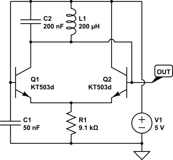
I've found this schematic of a LC sine wave producing circuit online, and I was trying to figure out how it works (particuarly the feedback cycle).enter image description here

Can someone tell me if this is right? I think I've figured it out to a point, but I'm not completly sure. Alot of the details on these circuits are quite fuzzy and dont really explain much. (When describing points on the schematic, I will use terms like "the top of the C1" to describe the part of the capacitor that appears closest to the top of your screen).

1: L1 begins to build a field, and as the current through L1 and Q2's gate rise, Q2 begins to open up and produces the beginning of a sine wave with a positive slope. At the same time, C1 is charging as well.

2: L1 begins to become saturated and the current remains constant, Q2 is almost completely open. The sine wave has just about reached its crest. C1 is near the end of charging and therefore Q1 begins to open up.

This is where I can't figure anything else out. How does the capacitor and inductor actually oscillate to produce this sine wave? It somewhat makes sense, but I cannot grasp the full concept when I try to fully analize the circuitry. Any help is appreciated. Thanks.

\$\endgroup\$

4 Answers 4

5
\$\begingroup\$

Q1 and Q2 are actually cross coupled because each transistor has its collector tied to the opposite transistor's base. This can be looked upon as a form of dynatron oscillator because R1 behaves like a constant current source. Where efficiency is more of a concern a choke is used for R1. If you tip the circuit upside down and redraw with PNP transistors then all will be clear to you.

There should be a cap across the inductor and the expected frequency is predictable. C1 is just a bypass cap and does not determine the osc frequency. Normally the output is taken from the junction of Q1 collector, Q2 base, and L1. Taking the output from where it's taken will give less output and lots of second harmonic distortion. This unorthodox output point may be useful if a frequency doubler is to follow.

\$\endgroup\$
3
  • \$\begingroup\$ Could you please draw where the capacitor "accross the inductor" should connect to exactly? Its it exactly parallel to the inductor and leaving everything else as is? I wish I could draw it into your answer, but I don't want to vandalize your answer with something that might be wrong! \$\endgroup\$ Commented Nov 20, 2019 at 20:27
  • 1
    \$\begingroup\$ @GuntherSchadow The cap can go across the Coil \$\endgroup\$
    – Autistic
    Commented Nov 20, 2019 at 20:30
  • \$\begingroup\$ would you look at my answer below and see if you can correct and put the schematics into yours? I love this circuit so much for its simplicity, but wan to make sure it's right. Mine should do a frequency of about 25.165 kHz \$\endgroup\$ Commented Nov 20, 2019 at 21:08
2
\$\begingroup\$

This is an attempt to edit @Autistic's answer above, as it's great eye opener but doesn't actually show the schematics. I don't want to draw into @Autistic's answer. But I am glad if someone steals and corrects my drawing and puts it in.

To me the eye opening points were:

  1. "Q1 and Q2 are actually cross coupled because each transistor has its collector tied to the opposite transistor's base."
  2. "There should be a cap across the inductor and the expected frequency is predictable. C1 is just a bypass cap and does not determine the osc frequency."
  3. "Normally the output is taken from the junction of Q1 collector, Q2 base, and L1."

So there, I drew this:

schematic

simulate this circuit – Schematic created using CircuitLab

What I've tried to accomplish with my drawing is to show the symmetry. But it might not be right because I do not know what exactly @Autistic meant with the statement 2. in the summary list above, where exactly that other capacitor goes.

If the CircuitLab was more powerful with re-routing connections while we move components around, I could improve this more like horizontally flip the entire schematics around so the voltage source would be on the left.

\$\endgroup\$
2
\$\begingroup\$

In the same idea as Gunther Schadow I propose the following presentation of a similar schematic.enter image description here

C1 is irrelevant to the operation of this circuit since it is in parallel with a zero ohm power source. You could take C1 out and it would make no difference in the circuit performance, at least that is true in theory. In practice, no power supply is ever zero output impedance, hence a 50nF cap in parallel will absorb high frequency voltage disturbance of that supply.

C3 C4 are the representation of input capacitance for Q3 Q4. ( values are approximate only)
C2 represent the output capacitance for Q3 Q4. Since both Base and Collector are connected on 2 nodes only, it appear that both output capacitance are in parallel, so they become 1 capacitor. And, since C3 C4 are in series, they can be viewed as 1 capacitor between both Base. So then, in essence, ( C3 series C4 ) in parallel with C2 = 1 only capacitor. We then end up with 1 only capacitor in parallel with L2, creating an LC tank. Because both Q3 Q4 are mounted as a multi-vibrator tied by this LC tank, all elements are present to initiate an oscillation.

R1 is replaced by R1 R2. Just to better visualize that notwithstanding the power supply ties this circuit is free to oscillate. DC wise the supply feed current into both collectors and bases equally since L2 is zero ohm for DC current. DC wise it’s as if we had both transistors in complete parallel Base1 connected to Base2, same for emitters and collectors. Furthermore, both bases and collectors are connected together. Meaning that the DC current flow equally through both transistors (theoretically).

Since the output capacitance of the transistors are subject to a non linear impedance (transistor intrinsic diode effect from base to emitter) the LC tank is disturbed by the non linear current voltage curve created. More voltage supply create more base current, hence parasitic capacitances are charged discharged faster, creating a change in oscillating frequency. The more current the higher the frequency, consistent with lab result ( at least that’s how I view it, but perhaps this may be a bit of a non scientific explanation )

\$\endgroup\$
1
\$\begingroup\$

First off, it helps if you include a link to the source. According to that, Q1 acts as a common-base amplifier and Q2 acts as a common-collector amplifier.

In this circuit, C1 is connected directly to the 5V DC source, which means it is always at 5V. It actually has no influence whatsoever on the circuit. In real life, it's probably a bypass capacitor. In the simulation, you can remove it with no change in behavior.

I tried simulating it in PartSim, but the behavior is rather odd. At the start, Q1 turns on and Q2 stays off. The inductor current (and thus the Q1 collector current) is zero. Q1's base-emitter junction acts like a diode, allowing current to flow from V1 to the resistor. VCE is almost zero, so the inductor voltage is equal to the B-E diode drop.

The inductor current rises at a constant rate. At the same time, the base current drops as Q1 starts acting less like a diode and more like an emitter follower. Their sum (the resistor current) is constant. About a quarter of the way through the cycle, the base current goes negative. (!!)

After a while, Q1 turns off. The inductor voltage polarity flips, raising the voltage of the middle node above V1. The B-C and B-E junctions in Q2 are both forward-biased, with B-E producing R1's current and B-C carrying the rest of the inductor current. With a constant voltage across it (the B-C diode drop), the inductor current falls at a constant rate, eventually going negative. (!!) Eventually, Q2 turns off and Q1 turns on, restarting the cycle. The output is a clamped square wave with an amplitude of about 600mV.

The current waveforms for the two transistors look pretty similar, so I'm skeptical of the source's description. Autistic's cross-coupled oscillator explanation sounds a lot closer, but your circuit is missing the capacitors, only has one inductor, and Q2's collector is AC-grounded. Compare this, for instance:

Cross-coupled VCO circuit

I don't understand why the inductor current starts flowing through Q1's C-B junction, or why the Q2 B-C/inductor voltage remains constant even after the inductor current reverses. Perhaps the junction capacitance plays a role, somehow? Regardless, it does seem to oscillate. Maybe someone else can figure this out. Here's my transient simulation showing start-up and a full cycle.

Transient sim Light blue = Q1 collector voltage

Black = output voltage

Light green = Q1 collector current

Orange = Q2 collector current

Purple = Q1 base current

Red = Q2 base current

Yellow = R1 current

Dark green = inductor current (into top pin)

\$\endgroup\$

Your Answer

By clicking “Post Your Answer”, you agree to our terms of service and acknowledge you have read our privacy policy.

Not the answer you're looking for? Browse other questions tagged or ask your own question.