0
\$\begingroup\$

I am in the process of writing a driver for the Intel 8259A PIC and using the corresponding datasheet for reference.

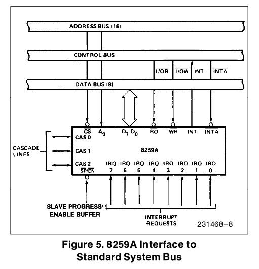
The datasheet contains a picture of the controller and its connection to the system bus:

Connection To the System Bus

I roughly understand the pins and connection but I cannot wrap my head around one: the A0 line.

It has two descriptions in the datasheet. The first one is as follows:

A0

This input signal is used in conjunction with WR and RD signals to write commands into various command registers, as well as reading the various status registers of the chip. This line can be tied directly to one of the address lines.

Taking a look at the ICWs (Initialization Command Words), I can understand how the A0 is used to "[...] write commands [...]." Address lines are designated with a leading "A" and a trailing number, which equals their position in the array of address lines, beginning at 0. Therefore, A0 means the very first address line of the address bus.

But address lines are used to address primary memory, that is, RAM. The Intel 8259A does not access RAM directly, though.
So why is that bit called A0 and how can it "[...] be tied directly to one of the address lines [...]"?

And why 0, specifically, if the second description says this:

A0 ADDRESS LINE: This pin acts in conjunction with the CS, WR, and RD pins. It is used by the 8259A to decipher various Command Words the CPU writes and status the CPU wishes to read. It is typically connected to the CPU A0 address line (A1 for 8086, 8088).

(2nd emphasis added.)

So, it's A1 for x86 and A0 for those other 8259A-compatible processors only? Why A1 for x86 then? That means powers of 2, which I do not see the use for in this context.

What's the purpose of that A0 bit and its name here?

\$\endgroup\$
9
  • \$\begingroup\$ Why are you studying the 8259? It's an obsolete part and not even carried by Digi-Key, Mouser etc. anymore. You're learning pretty useless material. Your link for the datasheet is bad and I can't find one elsewhere. Is this for school or are you trying to fix or build a retro computer? \$\endgroup\$
    – tcrosley
    Commented Mar 28, 2016 at 21:55
  • \$\begingroup\$ @tcrosley I updated the link (straight to MIT now), hope it's better now. I love those old PCs and just want to write some low-level code. This is all preliminary stuff, tough; I am definitely going to get to the APIC and that modern stuff but I guess the 82093AA I/O APIC datasheet just scared me off. I'll stick to that simpler stuff first, continue with more modern stuff (maybe first a VGA and APM driver), then some ACPI stuff but this might take a (long) while and so on. \$\endgroup\$
    – cadaniluk
    Commented Mar 28, 2016 at 22:01
  • \$\begingroup\$ @tcrosley ... And it's neither: I just read a datasheet and write old software on my Intel Core i5. I have too much time, I guess. \$\endgroup\$
    – cadaniluk
    Commented Mar 28, 2016 at 22:01
  • \$\begingroup\$ It has something to do with A0 normally being used for CS on 16-bit controllers driving an 8-bit device like the 8259. \$\endgroup\$ Commented Mar 28, 2016 at 22:03
  • 1
    \$\begingroup\$ @cad, it was my very subtle way of trolling for members. \$\endgroup\$
    – user65586
    Commented Mar 28, 2016 at 23:01

1 Answer 1

2
\$\begingroup\$

The A0 line is not used as a real port address line (for addressing the chip select anyway), therein lies the confusion. It is used to differentiate between certain commands inside the 8259.

On page 4 of the datasheet it says,

A0 This input signal is used in conjunction with WR and RD signals to write commands into the various command registers, as well as reading the various status registers of the chip. This line can be tied directly to one of the address lines.

On page 13 of the datasheet, it shows that A0 is used to address one of internal registers (OCM1) instead of registers OCW2/OCW3.

I/O in the x86 computer is done using a special address space reserved for I/O ports. Various peripherals were typically not give a single address, but rather a range of addresses (a block) The first PIC (peripheral interrupt controller, i.e. 8259) was allocated addresses 0x20 to 03F, and the second one was allocated 0xA0-0xBF.

The high order bits of the block, namely A5 through A7 in this case, would be fed into an address decoder and generate the chip select signal. This left the low order five bits to be used by the peripheral as it pleased. In this case, the A0 bit was used by the 8259A. In the x86 the "real" bit A0 was used to distinguish between various registers (for example, OCW2 vs OCW3, when A0=0). So the A0 line had to be wired to something else, was wired to A1 instead. Since the decoded address bits for the first 8259 were 0x20 and 0x21, setting bit A0 for the 8259 would be done using port address 0x22 or 0x23 (A1 bit set).

\$\endgroup\$
7
  • \$\begingroup\$ Wait, but the ports of the master PIC, for example, are 0x20 and 0x21. So how does 0x22 fit in here? And what do you mean "The A0 line is not used as a real port address line [...]"? If it is not, how can one assert it then? \$\endgroup\$
    – cadaniluk
    Commented Mar 29, 2016 at 0:06
  • \$\begingroup\$ It is asserted as part of the address (using port addresses 0x20 and 0x21 for it not asserted, and addresses 0x22 and 0x23 for it asserted. So bit A1, with a placeholder value of 2 (A0 is a value of 1) is added to the address 0x20 or 0x21. \$\endgroup\$
    – tcrosley
    Commented Mar 29, 2016 at 0:20
  • \$\begingroup\$ OK, but some commands require A0 (A1 for x86) to be set. Would that not, for the base address 0x20, access I/O port 0x22? And what do you specifically mean "placeholder"? Maybe that would clear things up a bit for me. And if it is "asserted as part of the address," then how is it "not used as a real port address line"? \$\endgroup\$
    – cadaniluk
    Commented Mar 29, 2016 at 0:26
  • \$\begingroup\$ There is no port 0x22. Remember, I said the 8259 was allocated a block of 32 addresses from 0x20 through 0x3F. It actually decoded only two, 0x20 and 0x21. Yes, A1 is a real address line, but it is not part of the decode used to assert the chip select line. \$\endgroup\$
    – tcrosley
    Commented Mar 29, 2016 at 0:28
  • \$\begingroup\$ Alright, alright, I'm getting closer. Two more questions: (1) How can "[i]n the x86 the 'real' bit A0" be used to "distinguish between various registers" if "A0=0" as in your "OCW2 vs OCW3" example? Distinguishing seems only possible to me if different values can be assigned. And (2) if "setting bit A0 for the 8259 would be done using port address 0x22 or 0x23" but these are inaccessible because not used by the 8259A, how does the controller see A0 (A1) is set at all? \$\endgroup\$
    – cadaniluk
    Commented Mar 29, 2016 at 0:47

Your Answer

By clicking “Post Your Answer”, you agree to our terms of service and acknowledge you have read our privacy policy.

Not the answer you're looking for? Browse other questions tagged or ask your own question.