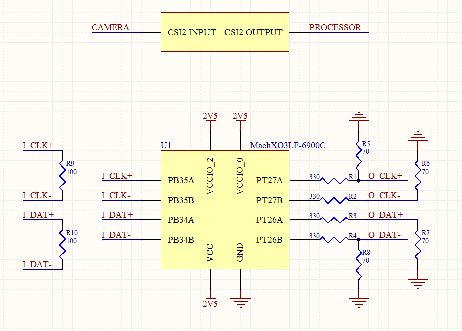
I would like to design a MIPI CSI2 bridge with a MachXO3L.
I leverage the LVDS25 input/output of this FPGA family with the adequate resistors for HS traffic. (I think) I don't care about LP as the camera is free-running clock and doesn't handle LP.
This Lattice document explains what I have been following: http://www.latticesemi.com/~/media/LatticeSemi/Documents/ReferenceDesigns/JM/MIPIDPHYInterfaceIP.pdf?document_id=50110
I don't want to deserialize/re-serialize data as the CSI2 traffic speed might be faster than what the MachXO3L can handle digitally. I want to achieve an "analog" bridge. Analog is perhaps not the right term, this is more by opposition to digital with deserialization/re-serialization.
My code looks like the following:
BLOCK RESETPATHS ;
BLOCK ASYNCPATHS ;

LOCATE COMP "clk_x1" SITE "C8" ;
FREQUENCY PORT "clk_x1" 12.000000 MHz ;
IOBUF PORT "clk_x1" PULLMODE=NONE IO_TYPE=LVCMOS25 ;


LOCATE COMP "I_CLK" SITE "R11" ;    # PB35A
#LOCATE COMP "I_CLK_N" SITE "T12" ; # PB35B

LOCATE COMP "I_DAT0" SITE "R13" ;   # PB34A
#LOCATE COMP "I_DAT0_N" SITE "T14" ;    # PB34B

IOBUF PORT "I_CLK"  PULLMODE=NONE IO_TYPE=LVDS25 DIFFRESISTOR=100 ;
IOBUF PORT "I_DAT0" PULLMODE=NONE IO_TYPE=LVDS25 DIFFRESISTOR=100 ;


LOCATE COMP "O_CLK" SITE "D10" ;    # PT27A
#LOCATE COMP "O_CLK_N" SITE "E10" ; # PT27B

LOCATE COMP "O_DAT0" SITE "F9" ;    # PT26A
#LOCATE COMP "O_DAT0_N" SITE "E11" ;    # PT26B

IOBUF PORT "O_CLK"  PULLMODE=NONE IO_TYPE=LVDS25 ;
IOBUF PORT "O_DAT0" PULLMODE=NONE IO_TYPE=LVDS25 ;
and also:
module csi_bridge(
    input clk_x1,

    input I_CLK,
    input I_DAT0,

    output O_CLK,
    output O_DAT0,
);

assign O_CLK =  I_CLK;
assign O_DAT0 = I_DAT0;

endmodule
I have tried various things but the processor can't manage to decode the traffic. Obviously, without the FPGA in-between, the processor can decode data.
On the scope, I see things moving on the output side, trying to mimic the input. My scope is not super high bandwidth so I must admit that I have some trouble to say what's really wrong.
Any idea what I should do and what I could be missing? Are they specific Lattice Diamond settings that I should look into?
** EDIT 1 **
To give further details, my objective in the end is to replicate a similar logic to Fairchild FSA642: https://www.fairchildsemi.com/datasheets/FS/FSA642.pdf. I have deeply tested this chip and I'm 100% sure that they don't deserialize/reserialize data because I have swapped clock and data, and it's still working. I'm wondering if I should not remove all resistors and consider all pins independently with an assign logic. Without any pull-up, voltage out won't go higher than voltage in.

