6
\$\begingroup\$

I'm just starting to learn SystemVerilog and work with FPGAs, and so far I haven't found a satisfactory way to test my code. I'm coming from a software background, and I have always been writing thorough automated tests for my code. I have been using JUnit-style frameworks (with lots of domain-specific wrapping on top, to reduce boilerplate), as well as QuickCheck-style frameworks, and found ways to use these frameworks to write concise test code that nevertheless provides me with high confidence in the product I'm developing. I haven't yet found anything equivalent for hardware description languages.

Introductory Verilog texts typically present testbenches that are just driving the input signals. These testbenches are unreadable repetitive walls of code (signal assignments) without assertions; these tests are not even automatic. Some texts try to incorporate machine-checkable assertions into the testbench code so that one does not have to look at waveforms to determine whether the test passed or failed. Still, the "wall of repetitive text" problem remains.

I researched the issue further, and found that the current industry standard for RTL verification is UVM. The idea does look better to me, I haven't looked in detail into it, but for me the big disadvantage of UVM is that UVM testbenches are not synthesizable.

If I can't run my tests on the actual FPGA, how can I be confident that my synthesized design works correctly? I understand that there is a high chance that it will work after the simulation tests have passed, but there are a lot of assumptions involved (that my code is not racy, that my code meets timing requirements, that the synthesis tool is correct etc.)

A parallel in the software world would be developing a program in C, compiling with gcc and testing it on x86 on Windows, and then compiling it with Clang and running it in production on ARM on Linux. The program should work, assuming that it does not have undefined behavior, does not have non-portable assumptions about the execution environment, both compilers don't have bugs affecting the program. This is a lot of assumptions that most software engineers would not make and instead would just run their tests on the production configuration.

Am I fundamentally misunderstanding something about real-world hardware design process? How are designs verified once synthesized into FPGAs and actual silicon? How to run existing test cases on designs in FPGAs and silicon?

Are there any industry-standard practices for synthesizable testbenches? Do people actually write synthesizable testbenches?

\$\endgroup\$
1
  • \$\begingroup\$ Your right in being paranoid about the final results. When I built ATE equipment using LabView I could write extra code as 'fake' inputs for simulation, but found myself building emulation boards with tiny versions of the real parts, and much lower voltages. But this gave me the real-time feed back I needed to be certain the software and the hardware would behave ok, and where I had to insert trim-pots and DIP switch's to fine-trim or put the ATE into a built-in test mode. At some point the 'standards' run out, or become very expensive. \$\endgroup\$
    – user105652
    Commented May 15, 2016 at 5:18

3 Answers 3

2
\$\begingroup\$

A general approach is to use more abstracted tests as you progress up the stack in terms of design complexity. Yes, you need to trust the tools (and the checking tools like logical equivalence proofs), but for a whole-fpga design (a) there won't be space for a testbench, and (b) exhaustive coverage will take a long time.

A good approach is to use exhaustive or random simulation testbenches at sub-module level, and more functional or vector based tests at full system level. For an FPGA which forms part of a complex design, you might end up needing to build a system emulator in hardware to drive the ports.

A suitable approach depends on your particular design, and how easy it is to generate test stimulus, capture the result and compare with the model (which might be simulation, or might be a higher level software model).

I think that due to the big variations in application, its hard to come up with a standardised approach. Sometimes FPGA is used to accelerate testing of the design, sometimes its the end product. Generally, you can trust that the resulting netlist (assuming it meets timing) will be honestly reproduced by the FPGA fabric - the abstractions are simpler than the transformations that apply in mapping C code to assembler code in the context of an OS.

\$\endgroup\$
1
\$\begingroup\$

I believe nothing beats testing on real hardware, and that applies to processors and FPGAs. I love working on microcontrollers with in circuit debugging because you can slowly iterate through the code and watch the results with real hardware/print statements, what have you. Even stepping through code on a microcontroller can be difficult because often you need the software to operate quickly so nothing is missed. In FPGA, there really isn't much in terms of "stepping" through code because it is all operating in parallel. You can attach an integrated logic analyzer and capture a moment in time and look how all the signals propagate over time. You can kind of step through processes with a simulator, but that's not really the same thing.

So back to your question, how do you know your HDL code is going to work properly inside your FPGA? Generally you do just like you mentioned: Write a testbench to stimulate the inputs and test the outputs, and when you build the design, if you meet timing and assuming everything is constrained properly, your design is then guaranteed to behave the way you wrote it. I caution you to only believe this 99% if you have weird things going on like clock crossing, metastability, as it's hard to accurately model what happens in these cases. You then build your confidence by making a stellar test bench: Test the normal cases, the edge cases, everything. After this, you may still be hesitant. Most of the big name FPGA vendors have special licenses you can purchase that give you post-build simulation models. These should be timing-accurate, so your design is verified beyond the behavioral simulation.

I believe most ASIC vendors spend a huge portion of their budget on the test/verification team. They basically do all sorts of simulations to try and ensure the design is bullet proof, so the ASICs are not bugged.

Like a circuit simulation, the accuracy depends on how accurate your models are. Some companies these days will provide you with a timing-accurate HDL model if their parts, so testing the interface can be done ahead of time.

Constraining your inputs and outputs properly is also a big deal. Nothing is worse than you inputting incorrect constraints and the tools tell you that the design will work, when really it wont. I've also had to write plenty of my own hardware models, having to sift through every detail of the datasheets...ugh

If possible, I try to insist that I am to be provided with representative development hardware. I tell the higher ups that they will save a ton of debugging time if I get the real deal up front.

\$\endgroup\$
1
\$\begingroup\$

You are overly concerned in my opinion. It comes down to trust. Do you trust that the gcc compiler will produce the exact assembly instructions that correspond to the C code? It is the same with the synthesis tools. You are relying on the fact that they have been tested before deployment. That is why they charge significant amount of money for them.

Furthermore, you do not just do RTL simulation. Tools nowadays have timing closure analysis, in order to make sure you do not have meta stability. If you ensure that you have completed the timing closure, you will not end up with timing violations in your design.

If you are still concerned with your design, there is the so called gate level simulation. The timings of your synthesized design are imported into your simulation, and are modeled appropriately. With this method you can see the actual delays as the signal passes through the logic.

If you are really paranoid, as you should be in ASIC design, there are formal verification tools, that prove your design functions as specified. You can check, for example, if your design is equivalent to a golden design that you know works.

What happens in industry is that we develop testing jigs for verification. This is a separate product for testing the product. Usually we also do a variety of tests. This is what I can think of off the top of my head:

  1. Bare PCB continuity by PCB manufacturer
  2. Assembled PCB test using flying probe
  3. Test jig

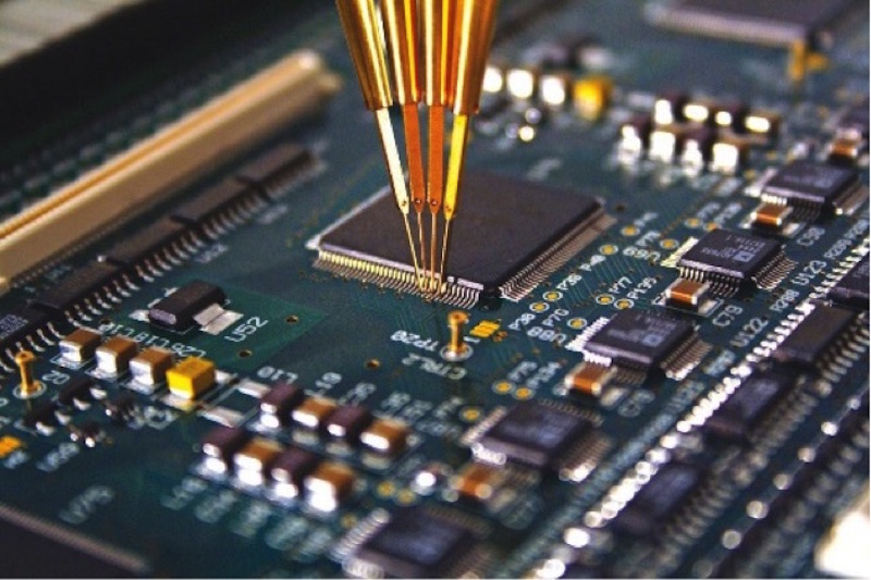
The flying probe is a machine that you program that probes the signals at different places on the PCB: flying probe The flying probe can program the board, apply voltages, and measure the outputs. It is slow compared to a custom testing jig. It also cannot deal with fast signals.

You should also be aware that by putting a test bench on an FPGA, you change the original design. I have had experience where putting the debugging modules on the FPGA reduced the maximum clock speed of the entire FPGA. This was caused by the longer routing required for the original design, not by the limitations of the debugger.

What does all that mean? Well, you are working on a hardware product. Hardware products require a proper testing strategy involving the entire team. The product can fail during test for a myriad of reasons, e.g. FPGA is not decoupled properly, and the power rail drops below the required voltage when executing a computationally intensive operation.

\$\endgroup\$

Your Answer

By clicking “Post Your Answer”, you agree to our terms of service and acknowledge you have read our privacy policy.

Not the answer you're looking for? Browse other questions tagged or ask your own question.