23
\$\begingroup\$

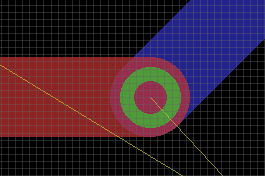
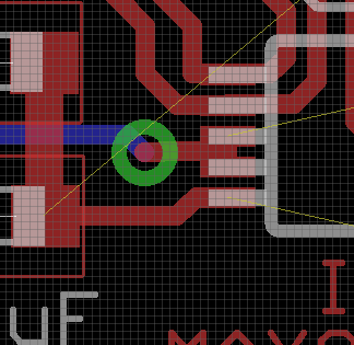
I am designing a two layer board, the problem is I do not know how to select via diameter and drill size, as well as outer and inner diameters.

In my circuit I use 056, 012 and 006 mil traces:

trace with 056 mil width trace with 012 mil width trace with 006 mil width

I have asked the manufacturer, they said they can make vias as small as 1 mil.

So my question is what should I choose for Outer, Inner diameter and drill size? For example, is it OK to use 10 mil drill for 6 mill trace? and what should it be for 56 and 12 mil tracks?

Also what is the green cylinder is going to look like when I get the board manufactured?

I am really short on money I can not afford to make mistakes.

\$\endgroup\$
6
  • 1
    \$\begingroup\$ You should ask the manufacturer about the via prices. If you go too small, there could be an extra fee. \$\endgroup\$ Commented May 22, 2016 at 9:12
  • \$\begingroup\$ @BenceKaulics the extra fee does not matter as long as I get the best result \$\endgroup\$
    – Dumbo
    Commented May 22, 2016 at 9:23
  • \$\begingroup\$ it's hard to guess "best result" without the full picture. but unless you have some special requirements, whatever looks good will work well. \$\endgroup\$ Commented May 22, 2016 at 9:41
  • 1
    \$\begingroup\$ For low current traces in DC and low frequency signals, the geometry of the via is mostly irrelevant. For high speed signals, the via's impedance must be considered, which is driven by its geometry. But that's a very complicated topic. \$\endgroup\$
    – Dan Laks
    Commented May 22, 2016 at 9:52
  • \$\begingroup\$ the green ring is the flange, it will be copper on both sides of the board, the centre of the ring is the plated drill drill hole, \$\endgroup\$ Commented May 22, 2016 at 9:57

3 Answers 3

28
\$\begingroup\$

The goal is to create a via with at least as much conductive area within the hole as the trace connecting to it (generally speaking, of course). My personal rule is to make the drill size diameter the same as the width of the trace, and the pad size roughly twice the diameter. This gives you a little bit of leeway in case your board is too dense to allow these sizes, and you need to adjust them. This is just a general rule that can be useful to beginners. It gives you a good size to shoot for.

Here is what completed vias look like on the board:

enter image description here

It is important to note that small vias will cost you quite a bit more than regular size ones. Generally I don't recommend going below an 8 mil drill. A microvia is a via that is less than 6 mil in diameter, and will cost you quite a bit more.

Physical size (beyond the 6 mil "microvia" limit) really isn't that important unless you need to consider current-carrying capability or controlled-impedance. Once these come into play there are a lot of things you'll need to consider such as plating type, plating thickness, plating length (thickness of your board), via positioning, etc. In basic designs, however, where you just need to bring one trace to another layer, I would suggest using 8 mil for all traces smaller than 8 mil, and for thicker traces use the trace width for the drill diameter. It's just a good rule of thumb.

\$\endgroup\$
7
\$\begingroup\$

The 'amount' of conductive material in the via should be equal (or more) to the amount of conductive material in the trace.

For example, lets say the trace is 12mil which is 0.304mm. Now, find a hole (via) with a perimeter of 0.304.

Some math: P=2*pi*r, 0.304 = 2 * pi * r --> r = 0.043mm --> d(iameter) = 2*r --> d = 0.096

A via of 0.1mm should be (theoretically) enough to deal with a 12mil trace. This assumes the via plating thickness is the same as the trace thickness, which is probably not valid, particularly for thicker boards. However, even doubling the 0.1 mm (4 mil) via diameter gives a pretty small hole. You must verify with the board house that they can drill such a tiny diameter and insert or plate a via so small. All board houses have a minimum hole diameter and slot width.

\$\endgroup\$
1
  • 2
    \$\begingroup\$ Of course, one might first ask the fab what the cost gradation is. Many specify a cliff size if you press them, where any size larger or equal costs nearly nothing, anything smaller will exponentially increase cost at each step. Most have the cliff at 0.2mm or 0.15mm, while often the maths show much smaller is fine for a design. Also some will do unlimited free vias as long as they are all the same size, but not if you keep switching sizes. \$\endgroup\$
    – Asmyldof
    Commented Dec 26, 2016 at 13:17
1
\$\begingroup\$

I came here with that same question, then I did some simple research and it became an answer :-)

Basically, my take is one should maintain the copper cross-section of the trace through the via in all directions, so on the same layer, and to the other layer(s) the via connects to.

I wrote a short article about this on Medium, which contains a link to a calculator I created on Google Sheets that takes your trace width as input, as well as the copper thickness, the hole's plating thickness, and some minima's as defined by your fab.

One key thing to consider is the plating thickness is much thinner than a typical 70 microns outer layer (2oz copper) and can go as low as 16 to 25 microns, requiring a relatively large drill diameter to get enough copper to match the cross-section of the trace.

TLDR: 1.5x trace width for the drill diameter, and drill + trace width for the pad, as a safe starting point accounting for thin plating.

\$\endgroup\$
1
  • 1
    \$\begingroup\$ Your article is behind a paywall. \$\endgroup\$
    – zud
    Commented Jun 8 at 16:16

Your Answer

By clicking “Post Your Answer”, you agree to our terms of service and acknowledge you have read our privacy policy.

Not the answer you're looking for? Browse other questions tagged or ask your own question.