2
\$\begingroup\$

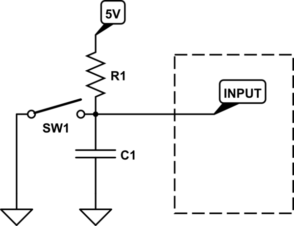
Often debouncing circuits are done like this :
schematic

simulate this circuit – Schematic created using CircuitLab

In this case, when switch is closed, C1 discharges in its internal series resistance, so discharge is very quick. If there is some rebounds and we suppose C1 internal resistance << R1, capacitor discharge time << capacitor charge time. Consequently, during rebounds when closing switch, response time will be very quick. I assume this configuration is useful when we a quick falling edge detection is required.

But, is this configuration safe for C1 lifetime?

\$\endgroup\$
1
  • \$\begingroup\$ The capacitor charge and discharge characteristics are slower than the transients generated during switch opening and closure, so those transients do not appear at the device input terminal. In other words, the capacitor and the resistances it charges and discharges through form low pass filters. \$\endgroup\$
    – Chu
    Commented Jun 3, 2016 at 8:00

1 Answer 1

1
\$\begingroup\$

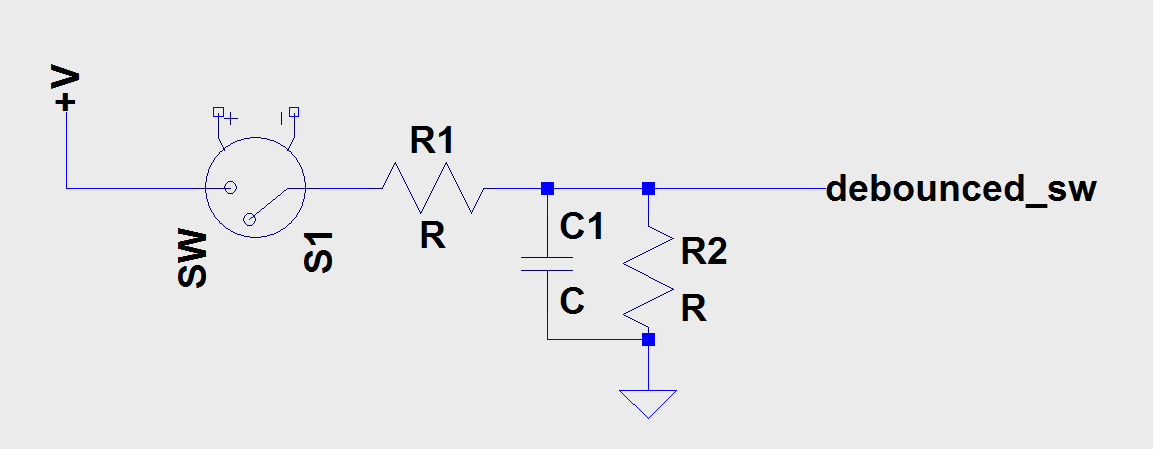
Your switch will wear out before your capacitor. The contact resistance and ESR+ESL in the capacitor will limit the peak current.

Your average plastic or ceramic capacitor can handle high peak current but you are wearing the switch from the arcing with high peak current, which is unessesary.

Would this be ok in your application: enter image description here

\$\endgroup\$
6
  • \$\begingroup\$ The issue with both circuits is that the input to the MCU (or whatever) sees a slow rise or fall time. Some MCUs can accommodate that, while others can't (a Schmitt trigger helps). These days, most debouncing is done inside the MCU, typically by firmware. \$\endgroup\$
    – Mark
    Commented Jun 3, 2016 at 7:53
  • \$\begingroup\$ Yes, if you can do debounce inside the MCU, either a hardware function within it or software, it's preferable. You need to choose R1 low enough to limit the current and C small enough to give you a resonable rise time and R2 small enough to discharge is fast enough. \$\endgroup\$
    – winny
    Commented Jun 3, 2016 at 7:55
  • 1
    \$\begingroup\$ The problem with that circuit is that the output signal is only a fraction (R2/(R1+R2)) of V+. \$\endgroup\$
    – JimmyB
    Commented Jul 22, 2016 at 11:12
  • \$\begingroup\$ @JimmyB R2 can be 100 ohm and R1 10 kohm. High enough to count as high. \$\endgroup\$
    – winny
    Commented Jul 22, 2016 at 11:39
  • \$\begingroup\$ @winny If R1 != R2 you get asymmetric charge/discharge times, hence different behavior for closing and opening the switch. \$\endgroup\$
    – JimmyB
    Commented Jul 22, 2016 at 12:52

Your Answer

By clicking “Post Your Answer”, you agree to our terms of service and acknowledge you have read our privacy policy.

Not the answer you're looking for? Browse other questions tagged or ask your own question.