4
\$\begingroup\$

As known there are two types DAC using R-2R ladder. One is voltage output and another is current output. The voltage output type has a constant output impedance which equal to R. The current output type has a input code dependent output impedance. Then how the output impedance dependent on the input code? Are there a mathematical function, such as $$R_{out} = f(n)$$ in which n is the input code, to show this?

Refs:

  1. http://www.analog.com/media/en/training-seminars/tutorials/MT-015.pdf
  2. https://en.wikipedia.org/wiki/Resistor_ladder
\$\endgroup\$

3 Answers 3

5
\$\begingroup\$

The output of a current-output R-2R ladder must be connected to a virtual ground, such as the inverting input of an opamp whose non-inverting input is grounded. Call the feedback resisor RF.

You can think of the circuit overall as "amplifying" the fixed VREF with a variable gain that is equal to

$$A = -\frac{R_F}{R_{OUT}}$$

and

$$V_{OUT} = -V_{REF}\frac{R_F}{R_{OUT}}$$

We know that

$$I_{OUT} = \frac{n}{2^N} \cdot \frac{V_{REF}}{R}$$

and

$$V_{OUT} = -R_F \cdot I_{OUT} = -R_F \cdot \frac{n}{2^N} \cdot \frac{V_{REF}}{R}$$

It's easy to set these two equations equal to each other and solve for ROUT:

$$-V_{REF}\frac{R_F}{R_{OUT}} = -R_F \cdot \frac{n}{2^N} \cdot \frac{V_{REF}}{R}$$

$$R_{OUT} = R \frac{2^N}{n}$$

When the input code is all-zeros, none of the R-2R legs are connected to the output node, so ROUT is infinite. When the input code is all-ones, ROUT is nearly equal to R.

It really doesn't matter, though, since as we said before, this output node needs to be connected to a virtual ground, so ROUT is in parallel with an impedance that is effectively zero. It's actual value has no effect on the rest of the the circuit.

\$\endgroup\$
4
\$\begingroup\$

To use either a voltage output R2R DAC or a current output R2R DAC properly you have to use it in such a way that the output impedance of the DAC does not matter.

For the voltage output DAC it is the same as how you would want to measure a voltage inside a circuit. You want to use a high impedance to measure it. So at the output of the voltage output DAC you will want to connect a high input impedance buffer amplifier, example:

enter image description here

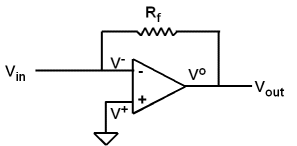
For the current output DAC it is the same as how you would want to measure a current in a circuit, you want to use an impedance as low as possible so that the current can flow through an impedance with the lowest voltage drop possible. Here you want to use a current input amplifier or a current to voltage converter. That can be a circuit as simple as:

enter image description here

This circuit has an input impedance of almost zero ohms. It multiplies the input current by the value of Rf and that will appear at the output as a voltage.

The trick with using such circuits is that it eliminates the influence of the (change in) output impedance of the R2R network. That way, you can forget about that output impedance also it does not introduce any errors anymore.

If you do not use an R2R DAC as I explained, the output impedance will matter and errors will be introduced.

Usually you can get reasonably small errors if you make the load impedance of the R2R DAC significantly higher (for voltage output) or significantly lower (current output) than the resistors used in the network. So if the network has 100 kohm resistors, for a voltage R2R load it with 10 M ohm. For a current output load it with 1 k ohm (so a factor 100 larger/smaller).

But the opamp solutions are more accurate !

\$\endgroup\$
1
  • \$\begingroup\$ I liked your second-to-last paragraph and expanded on that in my answer :) \$\endgroup\$ Commented Jun 5, 2016 at 13:01
2
\$\begingroup\$

I think I should expand on what Fake Mustache said about low frequency / DC design for DACs:

You do not generally prefer the opamp output stage. This gets increasingly important with the bandwidth of the signal you want to generate.

For example, see the schematic (p.1) of this high-rate DAC'ing software defined radio peripheral.

The idea behind these devices is that the DAC sits on the motherboard, and you use interchangeable daughterboards to take the generated signal, and filter it, mix it up to some RF, amplify etc it. That means the signal has to travel a bit and cross a connector before it reaches the relevant analog circuitry. Here, the design choice was hence to use a current DAC.

The AD9777 DAC's analog outputs get directly fed into the daughterboard connector:
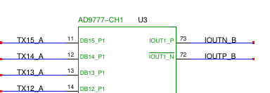
DAC output

dboard connector

Then, on the daughterboard (let's talk about the WBX here, schematic):
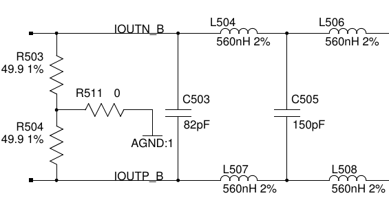
WBX input stage

we see that

  • we match the 50 Ohm of the transmission line, which is necessary to get the most energy out of the DAC into our daughterboard (and corollary, the least reflections/distortions and
  • no active parts whatsoever involved in buffering what the DAC produces.

So, the DAC here runs at 100MS/s, which means that it's already wise to not think of the signal as "current flowing through a piece of metal", but to layout the differential lines from DAC to connector as microwave lines, i.e. microstrip etc, and commit to the fact that the fields around these conductors will carry the energy. In this scenario, capable opamps are hard to find, harder to get linear and even harder to get linear enough not to waste expensive DAC bits.


Of course, a DAC for these rates is specced with an output impedance that allows for correct transmission line impedance and termination impedance design. Which also means that for the 50 Ohm termination used here, Analog guarantees driving capabilities. From the AD9777 datasheet, p. 46:

Note that the output impedance of the AD9777 DAC itself is greater than 100 kΩ and typically has no effect on the impedance of the equivalent output circuit.

hence, we're pretty much in the case where "ok, you've got a sink impedance in the range of 100Ω, but the source impedance is much much higher, so don't you worry". Of course, p. 47 also explains how you can use an Opamp as output buffer:
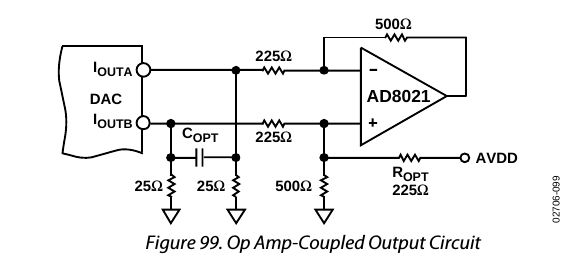
Opamp output stage

Yet the text mentions explicitly the disadvantages and design restrictions this has:

The common-mode (and second-order distortion) rejection of this configuration is typically determined by the resistor matching. The op amp used must operate from a dual supply since its output is approximately ±1.0 V. A high speed amplifier, such as the AD8021, capable of preserving the differential performance of the AD9777 while meeting other system level objectives (for example, cost, power) is recommended.

Since Opamps are never perfect, you infer a lot of additional problems. Just think about parasitic capacitance in the feedback line, inclucing the 500 Ohm resistor, or the fact that resistors and package pins have inductance, that change the phase of a signal depending on the signal's frequency... suddenly, your broadband DAC has a less-than-flat buffer, and changing that might not be trivial, lest you reduce the bandwidth to something manageable.

\$\endgroup\$
2
  • 1
    \$\begingroup\$ Actually I think you don't disagree with my answer but my answer refers only to the DC / low frequency case and you look at the case where the behaviour of the opamp limits the performance. So I think your answer is an addition to mine. \$\endgroup\$ Commented Jun 5, 2016 at 13:22
  • \$\begingroup\$ @FakeMoustache true. Will delete first sentence. \$\endgroup\$ Commented Jun 5, 2016 at 13:28

Your Answer

By clicking “Post Your Answer”, you agree to our terms of service and acknowledge you have read our privacy policy.

Not the answer you're looking for? Browse other questions tagged or ask your own question.