2
\$\begingroup\$

I'm trying to understand how the 74LS241 works. From what I read, if two input are high on a buffer, then the output will be high. For some reason, this isn't working on my circuit.

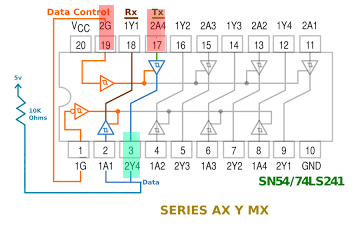
enter image description here

So here is what I did: I have put a led on the 3 output pin, in order to test the output. Then i wired the 19 and 17 pin with 3.5v, but my led isn't showing any high input.

enter image description here

(red where the input are at 3.5v, green where the expected output should be high)

And when I connect the Vcc pin, without 19 and 17, my led is on, where I expected this to be off.

I have the feeling that I have understood the schematic, but the fact is this is not working. So I clearly don't understand at all.

My question is: did i break the chip not protecting the input ? (I didn't put any resistors on the input). But I thought gate like those didn't need to be protected.

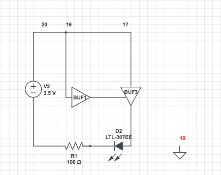
update Here is my actual scheme: enter image description here

\$\endgroup\$
11
  • \$\begingroup\$ What does "put a led on the 3 output pin" mean? HOW did you "put" the LED? Please show the schematic diagram. Your explanation "two input are high" sounds more like the definition of an AND gate. Do you understand WHY we have tri-state outputs? Do you understand what a buffer is and why we use it? \$\endgroup\$ Commented Jun 30, 2016 at 18:32
  • 1
    \$\begingroup\$ A 74LS241 (or any 74LS family part) will normally see an unconnected input as a High - you need to connect inputs directly to Ground to input a Low. Do you have 5 volts Vcc connected to pin 20, and have pin 10 grounded? \$\endgroup\$ Commented Jun 30, 2016 at 18:36
  • 1
    \$\begingroup\$ "diode like those didn't need to be protected" - what diode? \$\endgroup\$
    – Andy aka
    Commented Jun 30, 2016 at 18:50
  • 1
    \$\begingroup\$ There are both INVERTING and NON-inverting buffers. "Amplifier" implies linear/analog behavior. For that reason we don't typically use the word "amplifier" for digital/binary/logic systems. "Buffer" is the equivalent term for digital circuits. The logic IN (17) and tristate-control (19) inputs do NOT constitute an AND gate. And we still don't know how you have your LED connected???? \$\endgroup\$ Commented Jun 30, 2016 at 19:30
  • 1
    \$\begingroup\$ The minimum specified operating voltage for the 74LS (and other bipolar TTL) family is 4.5 volts. It is not guaranteed to operate at 3.5 volts. \$\endgroup\$ Commented Jun 30, 2016 at 23:18

2 Answers 2

2
\$\begingroup\$

A tristrate output can have 3 different states: low, high, or disconnected (also sometimes called 'floating', 'high-z'). In the first two instances the output is actively pulled low or high using a transistor; in the disconnected state, neither transistor is activated.

Pins 1 and 19 of the LS241 control this state for the buffers inside the chip. These 'G' inputs must be activated in order to have the buffers connected to them pull their outputs low or high, depeding on their input. Without it, the outputs float. Note the invertor symbol (tiny o ring) at the control gate connected to pin 1; you must pull pin 19 high to activate, and pin 1 low to activate.

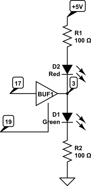
This circuit will help:

schematic

simulate this circuit – Schematic created using CircuitLab

If you pull pin 19 down, the output will float and both LEDs will glow dimly because current is passing through both of them. Pull pin 19 high, and the output will follow the input (17) and either the green or the red LED will glow brightly; the other one will be off.

\$\endgroup\$
4
  • \$\begingroup\$ thanks for the answer. This is clearly what I am expecting. for example: if I pull pin 1 down, and pin 2 high, I'm expecting pin 18 to be high. But my led at pin 18 just glow dimly and never change state, no matter if pin 2 is high or not connected. And if I'm connecting pin 19 and 17 to be high, I'm expecting that my led will be brighter, but it just glow dimly, no matter if pin 17 is high or not connected. \$\endgroup\$
    – Mr Bonjour
    Commented Jun 30, 2016 at 19:48
  • \$\begingroup\$ I was expecting that my led will be off with pin 17 not connected but pin 19 still high, and the led on with 17 and 19 high, but this is not happening. I was wondering if I didn't have broke my chip because I don't have protected the input gate, (but it wasn't asked in the schema). \$\endgroup\$
    – Mr Bonjour
    Commented Jun 30, 2016 at 19:49
  • \$\begingroup\$ @MrBonjour Try another gate then. Note that you may not enable both G inputs (e.g. pin 1 low and pin 19 high) at the same time if you connect the in- and output of the internal buffers. \$\endgroup\$
    – JvO
    Commented Jun 30, 2016 at 20:09
  • \$\begingroup\$ I have tried other gate (19 with 15, 13, 11) and I have the same behavior. I don't use the two G inputs at the same time. either one or the other. like if there are independant. \$\endgroup\$
    – Mr Bonjour
    Commented Jun 30, 2016 at 20:30
2
\$\begingroup\$

Unfortunately your test is invalid because (according to your recent schematic) your Vcc supply to the 74LS241 is only 3.5 V. This is outside of the allowed range for a normal 74LS device (normal 74LS power supply voltage is 5 V +/- 5% i.e. 4.75 V to 5.25 V). Therefore any results you get using a power supply of 3.5 V are not guaranteed to be those described in the datasheet.

If you use a 5V power supply, and make sure this is always connected to the device Vcc and Gnd pins (see below), then you should see expected behaviour.

And when I connect the Vcc pin [...]

So your first tests were done without any power connected to the Vcc pin! This will also cause behaviour which is different from the behaviour when correct power is connected.

I've done quite a lot of research since first writing this answer, and with unpowered 74LS devices and an input voltage between 0 V and 5.5 V, you may have "got away" without causing damage doing this - just resulting in a high impedance output, which would fit with the behaviour you described. You said:

I have put a led on the 3 output pin, in order to test the output. Then i wired the 19 and 17 pin with 3.5v, but my led isn't showing any high input.

Which I have interpreted as being:

You have [connected an LED + resistor between pin 3 and Gnd], in order to [view the state of] the output. Then [you connected 3.5 V to input pins 17 + 19, with nothing connected to Vcc pin 20] but [your LED didn't light despite the logic] high input[s].

This is not unexpected, since you didn't power the IC via its power pins for this test. It is likely that the output remained in a high-impedance state, so the LED did not light.

Then you said:

when I connect the Vcc pin, without 19 and 17, my led is on, where I expected this to be off.

Which I have interpreted as:

When you connected [3.5 V, as shown in your schematic, to] the Vcc pin, without [any connection to pins] 19 and 17, [your LED] is on, where [you] expected this to be off.

The LED being lit is not a surprise. Although it is not "best practice" to do this, unconnected LS TTL inputs will (usually) float high, as @PeterBennet has already kindly explained.

Therefore, although 3.5 V is outside of the power supply specification, we can expect input pins 17 and 19 to float high and behave as if they were connected to Vcc. Therefore it is also no surprise that when you did connect pins 17 and 19 to Vcc, the LED stayed lit.

Texas Instruments discusses some of these results of reduced voltage power supply voltages to ICs, in this short "Designing With Logic" document.

Unless you know exactly what you are doing and its consequences, do not apply voltages to the other pins of an IC, without the correct power supply voltage(s) also being supplied to its specified power pins (i.e. correctly connecting Gnd / Vss pins, as well as the Vcc / Vdd pins).

If you want to see more examples (related to modern CMOS devices rather than LS TTL) here are some other EE.SE topics where powering devices via other pins, instead of the power pins, caused unexpected behaviour:

\$\endgroup\$
3
  • 1
    \$\begingroup\$ Another issue I've observed is parts that behave as though pairs of pins are connected via PNP transistor, such that excessive voltage on one will cause the device to source current into the adjacent pin. \$\endgroup\$
    – supercat
    Commented Jun 30, 2016 at 22:05
  • \$\begingroup\$ @supercat - In case it is of any interest, I found some tech info which may be related to that behaviour you observed, in the TI document I mentioned in my updated answer, called "Designing With Logic", especially section 4 starting on page 8. \$\endgroup\$
    – SamGibson
    Commented Jul 1, 2016 at 1:22
  • \$\begingroup\$ I don't know that I'd actually seen a chip manufacturer document the behavior, but I've observed it and understood enough about silicon to understand that two P regions joined by an N region form a transistor. I would have guessed the current gain was more than 0.01, though. \$\endgroup\$
    – supercat
    Commented Jul 1, 2016 at 1:44

Your Answer

By clicking “Post Your Answer”, you agree to our terms of service and acknowledge you have read our privacy policy.

Not the answer you're looking for? Browse other questions tagged or ask your own question.