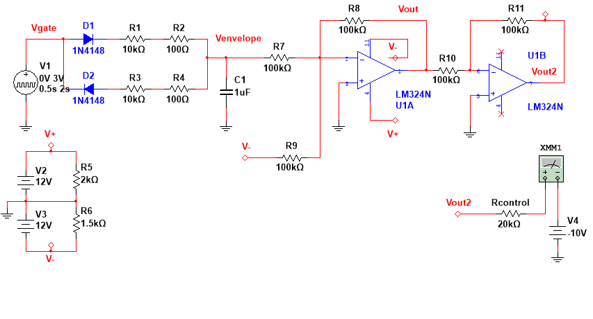
I am designing a transient generator for Eurorack style analog synthesizer equipment. This will generate a current envelope that will be the control input to a 13700 IC via its current control pin (pin 1). I have simulated this circuit in Multisim so far. My next step will be to breadboard it. However, I'd like to share the design here for any feedback anyone may have. Below is an image of the circuit.
How it works: when a note is "on" from the previous system, it will generate a voltage between about 2.8 and 4.5V. This is represented by V1. The diodes in series with resistors are for the attack (charging) or release (discharging) portions of the volume envelope. R1 and R3 will be 1Meg pots. R2 and R4 are resistance limiting resistors. When R1 is a large value, C1 will charge more slowly, and this will cause a "fade in" of volume to occur on a note that is played. A large value for R3 will cause C1 to discharge more slowly, and the note's volume will fade out more slowly.
The transient across C1 is summed with -12V. -12V will keep the 13700-based voltage controlled amplifier silent (its input pin is represented by V4). So, any increase in positive voltage will increase the volume of a note. The inverting summer will sum a voltage and -12V, e.g., +3 and -12 = +9. This value will be inverted, so U1B is a unity gain inverting amplifier. This would create -9V (from the example numbers given previously).
The maximum value of 4.5V would place about -7 V at Vout2, which would create about 160 uA leaving V4, which is my goal. V4 is the current control pin on a 13700 oper. trans. amp. I have measured with my setup that 160 uA will output a 10 Vpp output audio wave, which is what I desire. I will probably put a pot in series with Rcontrol so that the user can adjust the sensitivity to a control current here. Also, as some modules could have control outputs as high as 10V, if Vout2 = 2, the current out of V4 would still be below 2 mA, which is the max current it can tolerate sinking.
My next step is to breadboard this.
Can anyone identify any ways in which this circuit can be improved?

