19
\$\begingroup\$

I am not much of an electrical person but I'm trying to get an idea about it, so keep in mind I have very little background outside of college level electrical physics with calculus, and a strong basis in mathematical logic. I was learning about things you can make with logic gates and came across an adder. I like to give things a try before I look at the answer, so I came up with my own adder. The only difference between my adder and the one in the book I'm reading is that there's an OR gate at the end of their adder for the carry out wire, whereas I just put two wires together. It seems to me that putting two wires together is identical to an OR gate, as there is no electricity out of the node if there's no electricity in, and there is some electricity out of the node if there is some in from either or both sources.

My question is: What is the difference between putting two wires together and making a proper OR gate?

My guess is that it has something to do with the amount of electricity (current?) on the output wire from the 3-node/OR gate, but my understanding of circuits is a bit rusty. Thanks for your help!
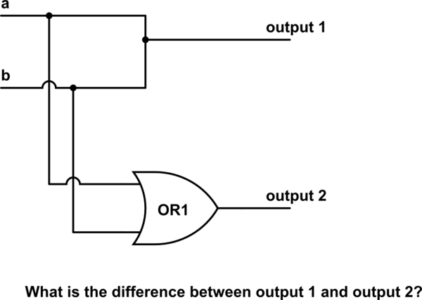
schematic

simulate this circuit – Schematic created using CircuitLab

\$\endgroup\$
1
  • 9
    \$\begingroup\$ If you used output 1, had "a" at 5V and "b" at 0V, congrats you made a short circuit. \$\endgroup\$
    – Bradman175
    Commented Jul 22, 2016 at 12:25

5 Answers 5

20
\$\begingroup\$

What you have to understand is how logic level H and L are represented. Both logic levels H and L are represented by two voltages, i.e. L does NOT mean floating potential or "not connected".

L means the voltage is (close to) 0V, i.e. connection to GND.

And of course H is indicated by a higher voltage, e.g. 5V, i.e. connection to positive supply voltage.

So if two digital outputs have different values (H and L) connecting them would cause a short circuit, not an OR gate.

In very most cases in digital logic connecting two outputs together is wrong.

Exceptions are

  • so-called tri-state outputs which can be in a third state "Z". Z actually means high impedance, i.e. "no connection" and
  • so-called open collector (or open drain) outputs which can be AND-wired (similar to what you wanted to do for OR). But then you need an additional pull-up resistor.
\$\endgroup\$
3
  • 1
    \$\begingroup\$ I would like to add another exception regarding connecting multiple outputs. It is common in VLSI for designers to use two of the same exact gate, with the same inputs and outputs shorted together. As long as the gates are physically close, it acts to double the drive power of the gate, which can be helpful if you don't have the desired drive level already. \$\endgroup\$
    – jbord39
    Commented Jul 22, 2016 at 15:53
  • 1
    \$\begingroup\$ @jbord39: thanks for the input; I thought about that too (e.g. several inverters in parallel to increase output current) but wasn't sure if this is good practice (because of possible differences in the gates e.g. differences of switching thresholds would cause increased current during switching). \$\endgroup\$
    – Curd
    Commented Jul 22, 2016 at 16:08
  • \$\begingroup\$ Yeah when I first started out and saw it I was wondering 'what is this?!?'. But apparently it is fairly common and has been done for quite some time. \$\endgroup\$
    – jbord39
    Commented Jul 22, 2016 at 16:12
10
\$\begingroup\$

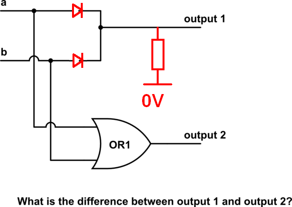
To avoid the two outputs "clashing" when one is high and the other is low, the simple two wires become a diode OR gate: -

enter image description here

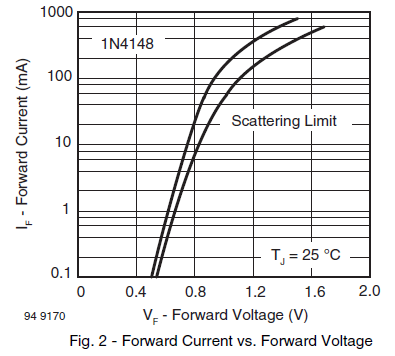
This usually works quite well but there is a slight (0.5V) degredation in the high voltage level reaching the output due to the forward diode volt drop. Here is the forward characteristic of a 1N4148 diode: -

enter image description here

If R is chosen to cause a current of about 0.1 mA then the volt drop will be about 0.5 volts.

\$\endgroup\$
7
  • 2
    \$\begingroup\$ Another restriction worth mentioning: the output can't be used as input to a wired-AND gate because of its high impedance at L. Therefore neither combination with another wired-OR gate (because of H voltage degradation) nor combination with another wired-AND gate (because of high L impedance) works. \$\endgroup\$
    – Curd
    Commented Jul 22, 2016 at 10:20
  • 1
    \$\begingroup\$ And speed? Due to the diodes' reverse recovery charge. \$\endgroup\$ Commented Jul 22, 2016 at 18:34
  • \$\begingroup\$ @PeterMortensen I never said it was perfect but it's a whole lot better than two wires joined together. \$\endgroup\$
    – Andy aka
    Commented Jul 22, 2016 at 20:00
  • 1
    \$\begingroup\$ Another issue with this setup is the voltage drop on the diodes. Unless the resistor is super-beefy, there is going to be some current. This means output1 will be some 1.x volts lower than the ideal logical high. This could ruin your day if you use LV CMOS. \$\endgroup\$ Commented Jul 22, 2016 at 20:13
  • 1
    \$\begingroup\$ Sorry that I missed it - but still, I would guess it's more than just 0.5V. \$\endgroup\$ Commented Jul 22, 2016 at 20:15
5
\$\begingroup\$

Can this work ?

This can work ONLY IF the LOW logic level in your circuit is represented as a none connected point [a point with no voltage with respect to any other point in your circuit], something like following circuit

enter image description here

So yes, your adder conceptually works BUT

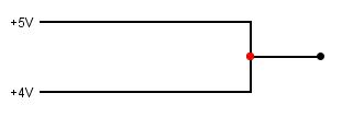
1- What if the two nodes are 'HIGH' but one of them is slightly higher voltage than the other?

enter image description here

A: given the fact that a very low resistive path exists between them, you will have a short circuit. A huge amount of current will flow that will burn your circuit

2- What if i want to interface this adder with other logic devices ? will it work ?

A: No it wont work, for example you cant interface this kind of adder with a CMOS digital device. So you need to build a library of digital modules that all works this way, you need to build your own AND,OR,NOT,NAND gates that all can work with this kind of logic.

3- What if we fixed this problem and represented the 'LOW' state as a 0 volts and the 'HIGH' state as - for example - 5 volts can we still interface this adder with a CMOS logic device?

A: No you cant because whenever one of the two nodes is HIGH and the other one is LOW you will have a short circuit, and a huge amount of current will flow that is enough to burn your circuit

So this kind of logic is only valid if you represent the 'HIGH' and 'LOW' with an LED or a light bulb [something visible] , but its not a practical way to implement complex circuits and storage devices using this kind of logic.

\$\endgroup\$
0
\$\begingroup\$

It is sometimes done in simple situations like relay logic (in cars, central heating systems etc.) Common features are that logical low is open circuit (not grounded) and input impedances are low (a relay's coil is it's own pull-down resistor). These two features go hand-in-hand.

Because teaching examples often use on-off switches as inputs and lamps as outputs, they may work in this fashion regardless of the point they're trying to make.

\$\endgroup\$
0
\$\begingroup\$

The basic reason for your "wire or" not being a workable option, is that the inputs are not isolated from themselves and from the output. Isolation is critical, for the proper operation of logic circuits.

\$\endgroup\$
1
  • \$\begingroup\$ "... the inputs are not isolated from themselves ..." - I think you mean "not isolated from each other. "Isolation" probably isn't the right word as it suggests galvanic / separate ground isolation whereas in fact they share the common power supply and are directly connected. To make this a good answer you would need to explain why "isolation" is critical. \$\endgroup\$
    – Transistor
    Commented Jul 30, 2016 at 8:16

Your Answer

By clicking “Post Your Answer”, you agree to our terms of service and acknowledge you have read our privacy policy.

Not the answer you're looking for? Browse other questions tagged or ask your own question.