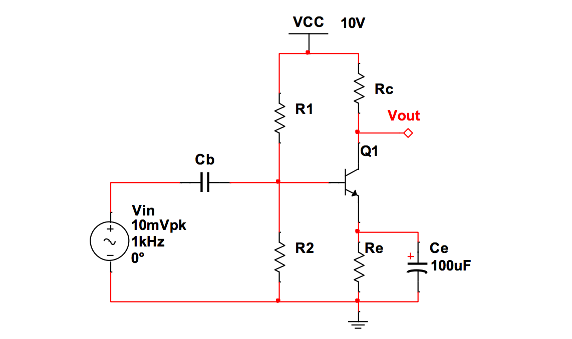
The goal is to set the quiescent (still, quiet, unmoving) current in such a way that \$V_{OUT}\$ has maximal room for signal swing, when it is applied. The idea here is to assume that if you set everything else correctly, the amplified signal will clip simultaneously on the top and bottom, if amplified too much. Think of it as a voltage band with a DC bias on it, within which the signal oscillates. But to set that band, you have to decide just how wide it is, first.
You are instructed to set \$V_E=1\:\textrm{V}\$. You are also supposed to figure out how much to also reserve for a minimum value of \$V_{CE}\$ on \$Q_1\$. In general, you need to keep \$Q_1\$ out of saturation. But the exact demarcation for that is a matter of what you consider important in the circumstances. Broadly, it must be the case that \$V_{CE}\ge 700\:\textrm{mV}\$, but there are lots of other considerations. I think \$V_{CE}\ge1\:\textrm{V}\$ in almost all circumstances, and more is better if you can afford it (Early Effect is only one reason why.) But in this case, you don't have any explicit guidance. So ignorant of that, I'd set the minimum \$V_{CEmin}=1\:\textrm{V}\$ and move on.
Now that you know these two things, or have decided them, you can figure out how much headroom you have left. This is:
$$V_{PP}=V_{CC} - V_E - V_{CEmin}=10\:\textrm{V}-1\:\textrm{V}-1\:\textrm{V}=8\:\textrm{V}$$
Now that you have that value, you take half that, or \$4\:\textrm{V}\$, as your midpoint within that range. Subtract this midpoint from \$V_{CC}\$ and you get a quiescent point, for the collector, of \$V_{C}=10\:\textrm{V}-4\:\textrm{V}=6\:\textrm{V}\$.
You are told to set \$I_Q=1\:\textrm{mA}\$. So it must then follow that \$R_C=\frac{4\:\textrm{V}}{1\:\textrm{mA}}=4\:\textrm{k}\Omega\$. I'd choose the standardized value of \$3.9\:\textrm{k}\Omega\$. (Given \$\beta=600, I_E\approx I_C\$.) It also follows that \$R_E=\frac{1\:\textrm{V}}{1\:\textrm{mA}}=1\:\textrm{k}\Omega\$.
You now have to set \$R_1\$ and \$R_2\$ correctly. If you don't, none of the above calculations are valid. For setting \$I_Q\$, \$Q_1\$ is operating as an emitter follower, so the biasing is important. Mistakes will mean that your assumed value for \$I_Q\$ is wrong and this will move the quiescent point of \$V_C\$. (It's not critical that you get this perfect. You just need to get it into the ballpark. A design that depends on perfection here is doomed, anyway, as parts vary quite widely.)
So, you make an assumption here that with a quiescent current of \$1\:\textrm{mA}\$, that \$V_{BE}=700\:\textrm{mV}\$ (we'll examine those assumptions at the end.) With that estimate, you know that the quiescent value for the base must be \$V_B=V_E+V_{BE}=1\:\textrm{V}+700\:\textrm{mV}=1.7\:\textrm{V}\$. You are told to make the biasing current about 10 times larger than \$I_B\$, which itself is 600 times smaller than \$I_Q\$ given the \$\beta\$ you were handed in the problem. This means about \$\tfrac{10}{600}=\tfrac{1}{60}\$th of \$I_Q\$. More is better, but you don't want to deviate much from the problem. So I'd pick \$20\:\mu\textrm{A}\$ as my value.
Given that this current is set so that it is about 10 times as large as \$I_B\$, you can roughly assume that all of this current flows through \$R_1\$ but that only 90% of it flows through \$R_2\$, as the base gets about 10% of it. So your resistor values are:
$$\begin{align*}
R_1&=\frac{V_{CC}-V_B}{20\:\mu\textrm{A}}=\frac{10\:\textrm{V}-1.7\:\textrm{V}}{20\:\mu\textrm{A}}=415\:\textrm{k}\Omega \\
R_2&=\frac{V_B}{0.9\cdot 20\:\mu\textrm{A}}=\frac{1.7\:\textrm{V}}{18\:\mu\textrm{A}}\approx 94.4\:\textrm{k}\Omega
\end{align*}$$
You can select standard values here, as well. You do not want to increase the values, as that would lower the currents further and, rather than stiffening the biasing, would weaken it. So I'd select \$R_1=390\:\textrm{k}\Omega\$ and \$R_2=91\:\textrm{k}\Omega\$.
FINAL NOTES:
The fact that \$C_E\$ exists as it does in your topology means that the AC gain will be as high as possible and based upon little-re, which is roughly speaking \$r_e=\frac{k T}{q I_E}\$. (That value, plus the frequency dependent impedance of \$C_E\$, divided into \$R_C\$ will be the gain.) This is, in general, a bad design unless there is global negative feedback surrounding this circuit, added later. It's also bad because it is highly dependent on temperature, varies with the instantaneous value of \$I_E\$, and varies with the frequency-associated impedance of \$C_E\$. With global negative feedback, it's often quite good, though. Just be aware, is all. (Also, the reason why \$V_E=1\:\textrm{V}\$ is a reasonable setting for the quiescent point is to mitigate the temperature impact on little-re, regarding the DC value of the quiescent current.)
Given the standard values used for \$R_1\$ and \$R_2\$, it may be instructive to now attempt a new estimate on the actual biasing point. We've made assumptions above about \$\beta\$ and \$V_{BE}\$, for example. And we've adjusted our resistor values in order to be standard ones. What impact does all this actually have? What happens if the values we've chosen include error, as well. For example, resistor values may be \$\pm 5\$%. And the BJT's \$\beta\$ might be off by a factor of 2.
The base current in the BJT is vital here. So we can take the Thevenin voltage, \$V_{TH}=V_{CC}\frac{R_2}{R_1+R_2}\$, and resistance, \$R_{TH}=\frac{R_1\cdot R_2}{R_1+R_2}\$, of the base biasing pair, and make the following calculation:
$$\begin{align*}
I_B&=\frac{V_{TH}-V_{BE}}{R_{TH}+\left(\left(\beta+1\right)\cdot R_E\right)}
\end{align*}$$
Knowing that value, we can then compute the base voltage as:
$$\begin{align*}
V_B &= R_{TH}\cdot\left(\frac{V_{CC}}{R_1}-I_B\right)
\end{align*}$$
or, as a function of the BJT parameters,
$$\begin{align*}
V_B\left(\beta,V_{BE}\right)&=\left(R_1\vert\vert R_2\right)\cdot\left(\frac{V_{CC}}{R_1}-\frac{V_{CC}\frac{R_2}{R_1+R_2}-V_{BE}}{\left(R_1\vert\vert R_2\right)+\left(\left(\beta+1\right)\cdot R_E\right)}\right)
\end{align*}$$
From the above, I get the following results for the value of \$V_B\$:
$$
\begin{array}{l@{}r@{}c}
& & V_{BE} \\
\begin{array}{l}
\\
\\
\beta
\end{array}
&
\begin{array}{r}
\\
\\
600 \\
300
\end{array}
&
\begin{array}{l}
{
\begin{array}{ccc}
600 \textrm{mV} & 650 \textrm{mV} & 700 \textrm{mV} \\
& & \\
1.754 & 1.759 & 1.765 \\
1.643 & 1.652 & 1.662
\end{array}
}
\end{array}
\end{array}
$$
You can see that a significant change in the estimate of \$\beta\$, by a factor of 2, does affect the base voltage by about \$100\:\textrm{mV}\$ in this case. So I'd expect that different BJTs would yield roughly on that order of variation on \$V_E\$ and therefore on \$I_Q\$ -- by about 10%. That will affect the setpoint of \$V_C\$ also by about 10% or \$400\:\textrm{mV}\$.
That's probably quite tolerable.

