4
\$\begingroup\$

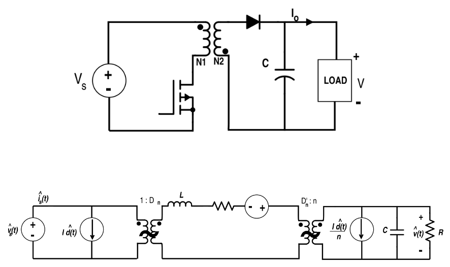
I am trying to derive the equation of small signal vout/d for a CCM flyback converter. In order to do this, I need the small-signal average model. I am having difficulty seeing how the small signal model for the flyback (or buck-boost) is derived from the flyback converter:

Flyback Converter and Small Signal Model

I recognize that the Vout/Vin for the flyback and buck-boost include a D in the numerator like a buck converter, and a 1-D in the denominator like that boost converter, and that is why the small signal model has a buck type stage (1:D) and a boost type stage ((1-D):1). I just wish to be able to be able to derive the small signal model directly from the normal circuit schematic.

\$\endgroup\$
2
  • \$\begingroup\$ One limitation comes to mind. Are you aware that it will only hold true for times/frequencies about 10 times the switching frequency since it's not a continous transfer? \$\endgroup\$
    – winny
    Commented Oct 25, 2016 at 13:29
  • \$\begingroup\$ That's fine, I plan to use the Vout/d transfer function to design the feedback network which will roll off well below the switching frequency. \$\endgroup\$
    – bears34
    Commented Oct 25, 2016 at 13:44

3 Answers 3

3
\$\begingroup\$

The control-to-output transfer function of this converter can be obtained by realizing that the flyback converter is an isolated buck-boost structure. You can analyze the buck-boost with different approaches like state-space averaging (SSA), current-injected control and the PWM switch model (to name the most-popular options). That latter is the simplest approach you can think of. It considers that the non-linearity in the switching circuit comes from the switching cell made of the power switch and the freewheel diode. Vatché Vorpérian who came up with the idea in 1986 considered the switching cell alone while leaving the rest of the linear elements (the L and C) untouched. You can thus analyze the isolated buck-boost converter by replacing the switching cell by the linearized PWM switch model and keeping the passive elements as they are. Exactly the same when you replace the transistor by its hybrid-\$\pi\$ model in a bipolar circuit This is the simplest and fastest approach. That being said, without any model, if you consider the dc transfer function of this flyback converter to be

\$V_{out}=V_{in}\frac{ND}{1-D}\$

then the quasi-static gain (control to output) of this converter is simply

\$H_0=\frac{dV_{out}(D)}{dD}=\frac{NV_{in}}{(1-D)^2}\$

Check out this PPT, it will guide you step-by-step in the process of determining transfer functions of switching converters:

http://cbasso.pagesperso-orange.fr/Downloads/PPTs/Chris%20Basso%20APEC%20seminar%202013.pdf

Good luck!

\$\endgroup\$
2
\$\begingroup\$
  • you are analyzing a coupled choke , not a transformer nor a 2 port circuit with linear transfer function.

The primary turns, \$Np\$ are selected to satisfy the AC voltage stress (volt-seconds) and the core AC saturation properties:

\$\frac{V\:T\:}{B\:Ae}=Np\$

  • Np is minimum primary turns
  • V is the maximum primary DC voltage (volts)
  • T is the maximum “on” period for Q1 (microseconds) B is the AC p-p flux swing (tesla) typically 200 mT for ferrite
  • Ae is the effective center pole area of the core (mm2)

Energy in the primary coil is transferred to the secondary coil during the "off" state of the flyback operation.

\$E = \frac{1}2LI^{2}\$ (joules)

\$V_{L} = (V_{i}-V_{o})D-V_{o}\$

  • then modulating duty cycle, \$D\$ with signal \$\delta\$ to get AC voltage \$v_L\$ on \$L\$

  • \$v_L = (V_i+V_o)\delta - V_o(1-D)\; ≈ (V_i+V_o)\delta \;\$

  • \$i_L = \frac {v_L}{j\omega L} = -j \frac{V_i+V_o}{\omega L}\delta \$

  • during the "off" state \$I_o=I_L (1-D)\$ then differentiating ac current with resulting \$i_L\$ having in-phase and 180' out of phase with \$\delta\$

  • \$i_o=-j\frac{(V_i+V_o)(1-D)}{\omega L}\delta -I_L\delta =-j \frac{V_i}{\omega L}\delta -I_Ld\$

  • The RHP Zero becomes \$ \omega_z=\frac{V_i}{LI_L}=\frac{R_oV_i^2}{LV_o(V_i+V_o)}\$

By using primary current sensing and current control loop, stability improves greatly.

  • I would like to give credit to above from one of the best SMPS designers I have briefly worked with in my past life as Test Eng Mgr at Burroughs.(mid'80's)

  • I hope this encourages you to buy one of his many books on the subject of SMPS Design... Tony

"in current, the immediate effect of trying to increase current is to cause a short-term decrease in output current. (This is a transitory 180° phase shift between cause and effect). This short transitory phase shift is the cause of the right-half-plane-zero in the transfer function. It is a non-compensatable dynamic effect and forces the designer to provide a very low-frequency roll off in the control loop to maintain stability. Hence transient performance will not be good. The flyback converter in the continuous mode has a boost-like converter characteristic and any converter or combination of converters that have a boost-type characteristic will have the right-half-plane-zero problem"

.

"The feature which makes it valuable for high output voltages is that it requires no output inductor. In forward converters, discussed above, output inductors become a troublesome problem at high output voltages because of the large voltages they have to sustain. Not requiring a high voltage free-wheeling diode is also a plus for the flyback in high voltage supplies."

.

"A further advantage for high voltage applications is that relatively large voltages can be obtained with relatively fewer transformer turns. " . "the discontinuous mode, with an inherently smaller transformer magnetizing inductance, responds more quickly and with a lower transient output voltage spike to rapid changes in output load current or input voltage. Second, because of a unique characteristic of the continuous mode (its transfer function has a right-half-plane-zero, which affects feedback loop stabilization), the error amplifier bandwidth must be drastically reduced to stabilize the feedback loop."

"Often, the effects of the layout, leakage inductance, output capacitor ESR, and circuit losses are unknown. As a result, it may be more expedient to measure the ripple current in the prototype unit and establish, or (if it has previously been calculated) confirm the final RMS values with CT's and true RMS meters."

Keith Billings, President of DKB Power Inc. and engineering design consultant, has over 46 years of experience in switch-mode power supply design. He is a Chartered Electronics Engineer and a full member of the former Great Britain’s Institution of Electrical Engineers (now the Institution of Engineering and Technology).

  • i.e. It will oscillate unless loop bandwidth is drastically reduced.
  • avoid saturation and flux walk or drift inside the BH loop for CCM.
\$\endgroup\$
1
\$\begingroup\$

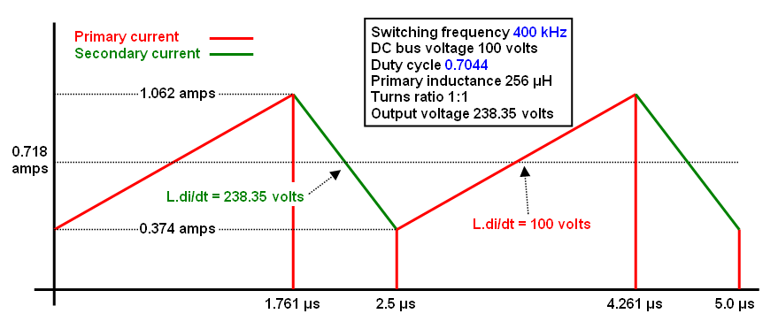
With CCM operation, the primary and secondary currents are constrained to be be inter-related like this: -

enter image description here

Picture source

The picture is for a 1:1 transformer running at 400 kHz. The primary current has to rise at a rate that is dictated by the primary inductance and applied voltage (Vin/Lp) and the secondary current has to fall at a rate dictated by secondary voltage and secondary inductance (Vout/Ls).

The average current is dictated by the average power consumed by the resistive load.

From the picture (and assuming the load resistance guarantees CCM) it is a simple case of recognizing that D (the duty cycle), Vin and Vout are related by: -

$$\dfrac{Vout}{Vin} = \dfrac{D}{1-D}$$

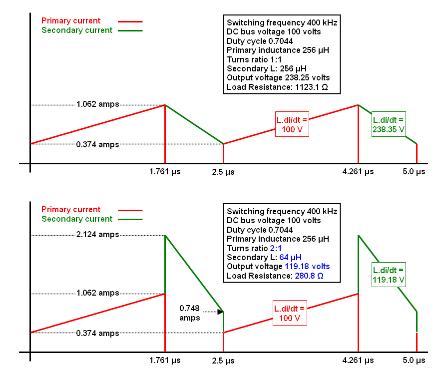
If the flyback transformer is a step-down type (N:1) then the formula becomes: -

$$\dfrac{Vout}{Vin} = \dfrac{1}{N}\cdot\dfrac{D}{1-D}$$

Picture: -

enter image description here

The derivation is just basic trigonometry and understanding that \$V=L\dfrac{di}{dt}\$.

\$\endgroup\$
0

Your Answer

By clicking “Post Your Answer”, you agree to our terms of service and acknowledge you have read our privacy policy.

Not the answer you're looking for? Browse other questions tagged or ask your own question.