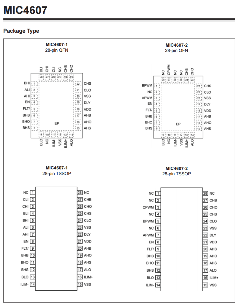
I have a part that's available as a TSSOP or as a QFN with an exposed thermal ground pad. I want to create a variants in Eagle for both packages. How can I show that the EP pad should be connected to GND without creating a new symbol?
2 Answers
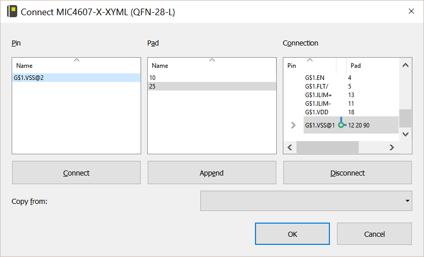
The append button can connect multiple physical pads with a single logical pin.
In addition to thermal pads, can be used to combine multiple VCC or GND pads together to appear as one pin in the schematic
You will need to clone existing package adding this pad to it. Ensure that you add pad with respect to spacing between pad and pins. After you do it, add this cloned package to existing device with different name to distinguish it, and connect this new pad as fkoran shown.
By the way, it is not clear if you really need this as a pad as soon as nothing will be soldered to it. You may consider using standard package without this ePad element, but when finishing ensure that space under the chip is filled with polygon connected to GND. The only difference will be that this way polygon will be covered by solder mask. But this may be not a good idea if chip is really heating hard.
Even more, to improve heat dissipation, I would add multiple vias under the chip. Look at page 34 and you will get what I mean.


