Glass is one of the best insulators when designing high voltage electronics, and correct me if I'm wrong, but capacitive touch screens work by measuring the charge of capacitors in a grid on the screens surface. The capacitors of a lower charge are closer to the point where someone is touching the screen. So, how does the glass on the surface of the screen not block the discharge of the capacitors into its human conductor? Is there some special type of glass used in these displays which has lower insulating properties than typical glass?
-
2\$\begingroup\$ The human is half of the capacitor, and the glass insulator is the dielectric. \$\endgroup\$– pjc50Commented Nov 9, 2016 at 22:27
-
\$\begingroup\$ @pjc50, this IS the answer and should be posted as an Answer, not as a comment. \$\endgroup\$– Richard CrowleyCommented Nov 9, 2016 at 22:29
2 Answers
Short answer: the glass is part of the capacitor.
Long answer:
A capacitor is at it's most basic level two conductors with an insulator in between them. Capacitance is everywhere, all objects in the world will have some level of capacitive coupling between them.
When a finger touches a capacitive touch screen a capacitor is formed between the finger and the electrodes in the touch screen. The human body and the ground plane of the device containing the touch screen are also capacitively coupled to the world in general. The result is that touching the screen increases the total capacitance between the electrode and the ground plane of the device.
This increase in capacitance is what the touchscreen detects.

simulate this circuit – Schematic created using CircuitLab
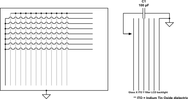
This is a 2 dimensional concept drawing of a 3 dimensional XY scanned capacitor grid for delta C changes resulting in xx mV changes of signal with the 100pF fingertip extended from a body of tens of thousands of body capacitance in series with picofarad series XY sensitivity.
- With series C equiv. cct., is the smallest C value which is modulated by the coupling factor of the finger thru the glass to the thin layer of ITO dielectric material that changes in a zone of XY scanned analog charge values.
