2
\$\begingroup\$

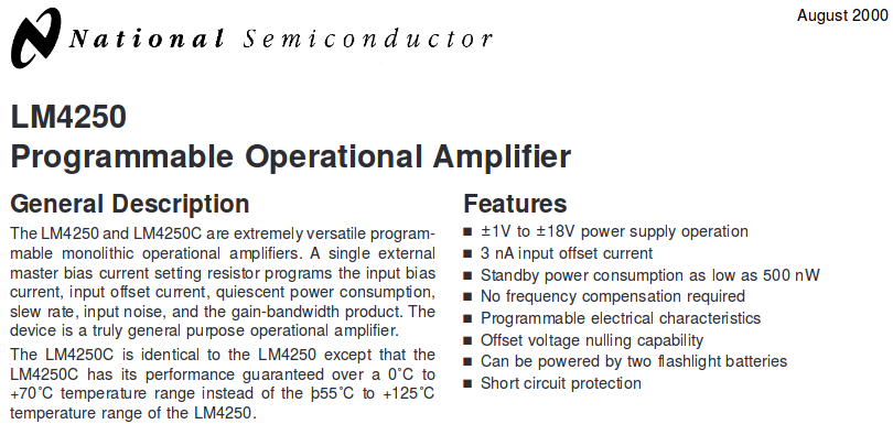
I am trying to understand the LM4250 op-amp. Datasheet:

http://www.ti.com/lit/ds/symlink/lm4250.pdf


Main description:

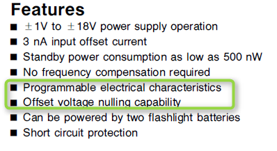
LM4250 description


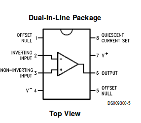
Pin-outs for DIP:

DIP pin-outs


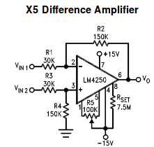
Example circuit:

LM4250 example circuit


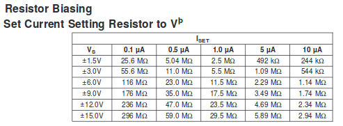
It appears that pin 8 (quiescent current set) can be used to change the quiescent current, according to this table:

Quiescent current table


My question is: why would you want to do this (change the current)? My understanding of quiescent current is that this is the minimum amount of current consumed by the device (not under load). Why would you want this to be any higher than the minimum the device is capable of?


Also, what is this symbol?

Unknown symbol

\$\endgroup\$
0

3 Answers 3

3
\$\begingroup\$

You would change the current in order to modify the tradeoff between performance (higher currents mean higher slew rates on internal nodes) and power consumption. That allows this single design to address a wider range of applications.

The odd symbol just seems to be another name for the negative supply (pin 4), which is where the other end of the resistor needs to go.

\$\endgroup\$
1
  • \$\begingroup\$ So basically the more power you give the chip (as higher quiescent current) then the more performance you get out of it, such as slew rate? That makes sense. \$\endgroup\$ Commented Jan 5, 2017 at 5:38
2
\$\begingroup\$
why would you want to do this (change the current)? 

For general purpose op amps, some performance parameters (noise and distortion in particular) tend to improve with higher current. Also the lowest quiescent current amps have severely limited bandwidth.[1]

The resistor(used to vary the current) is used to bias the LM4520.
enter image description here

This is used to vary the characteristics of the amplifier over a limited range.

A single external programming resistor determines the quiescent power dissipation, input offset and bias currents, slew rate, gain-bandwidth product, and input noise characteristics of the amplifier

. See section 3 in page #5 of the applicaiton note AN-71 Micropower Circuits Using the LM4250 Programmable Op Amp. here is the link.

The symbol is V-, the negative supply input (Pin 4).
The purpose is below:

In applications where the regulation of the V+ supply with respect to the V-supply (as in the case of tracking regulators) is better than the V+ supply with respect to ground the set resistor should be connected from Pin 8 to V-.

\$\endgroup\$
1
\$\begingroup\$

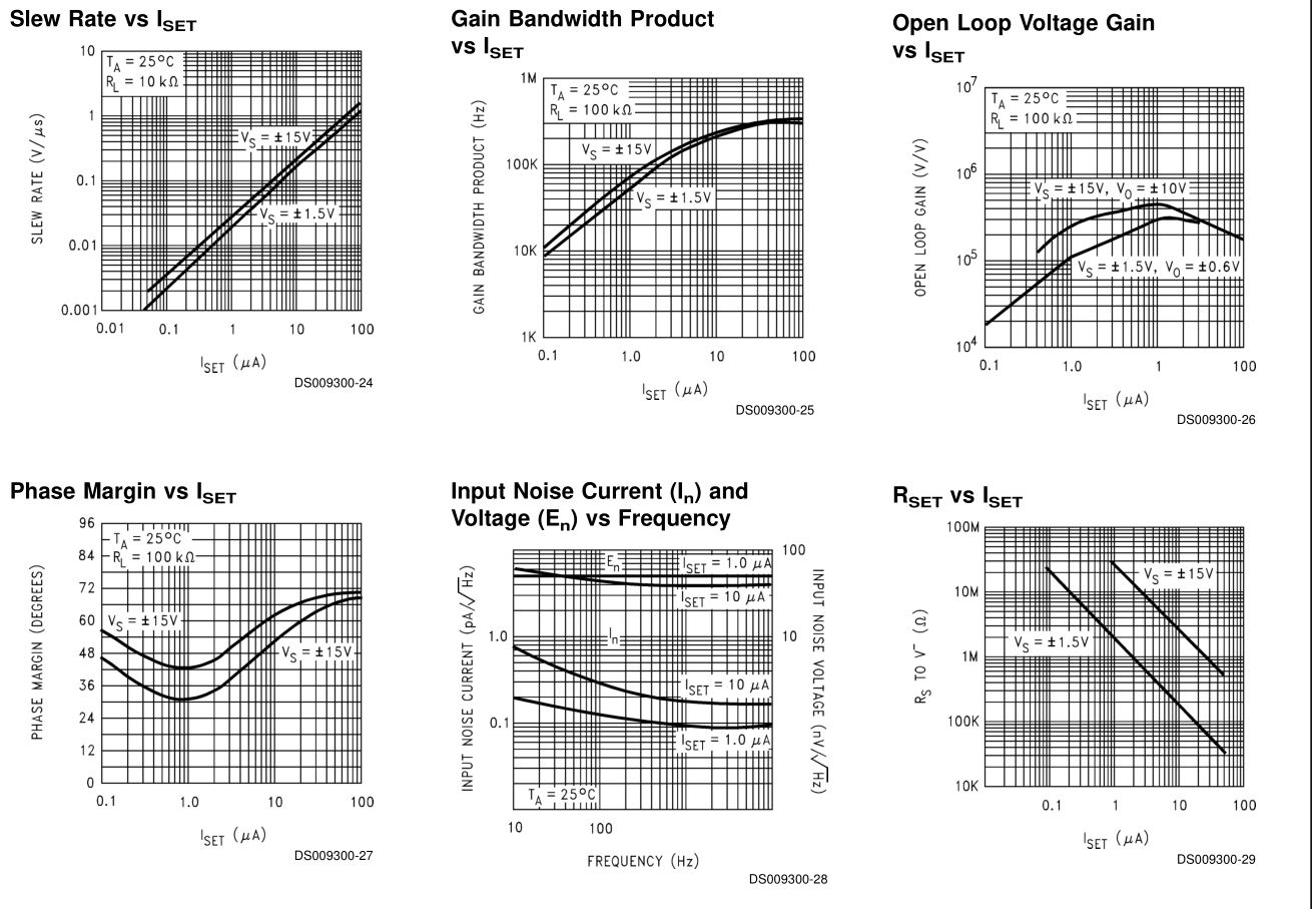
Tradeoffs for bipolar Op Amp Q current are;

- Slew Rate GBW Product, Open Loop gain, Input Noise current. enter image description here

\$\endgroup\$

Your Answer

By clicking “Post Your Answer”, you agree to our terms of service and acknowledge you have read our privacy policy.

Not the answer you're looking for? Browse other questions tagged or ask your own question.