I am building two PCBs, one which will house an MCU, WiFi, GPS, and other sensitive stuff. The second one will interface with solar chargers, batteries, and 12VDC loads.
The two boards will connect by I2C running over a short cable (1m or less), and I plan to use optical isolation to protect the more sensitive board, and a P82B96 to buffer.
This application note from NXP is very helpful, but I'm not clear how to properly adapt for my purposes.
My I2C bus is biased at 3.3V, operating at 100 kHz. Thus I require some combination of these two example circuits:
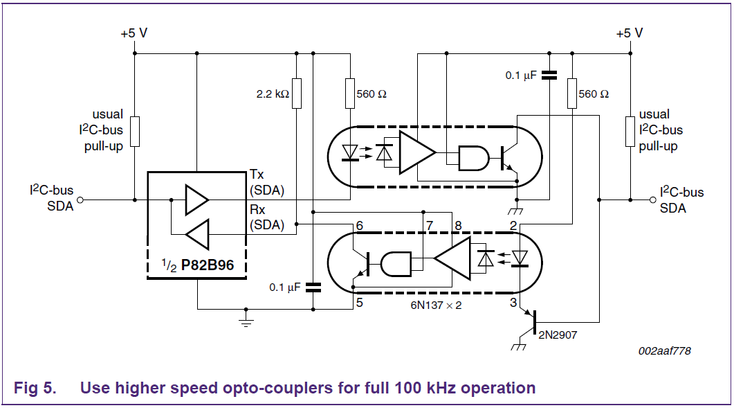
5V bias at 100 kHz:
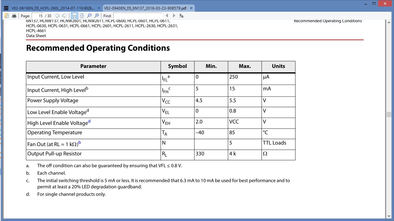
This diagram represents the speed I need, but since I'm changing from 5V to 3.3V, do I need to adjust the resistor values on the optoisolator? Also, is the choice of transistor affected by voltage?
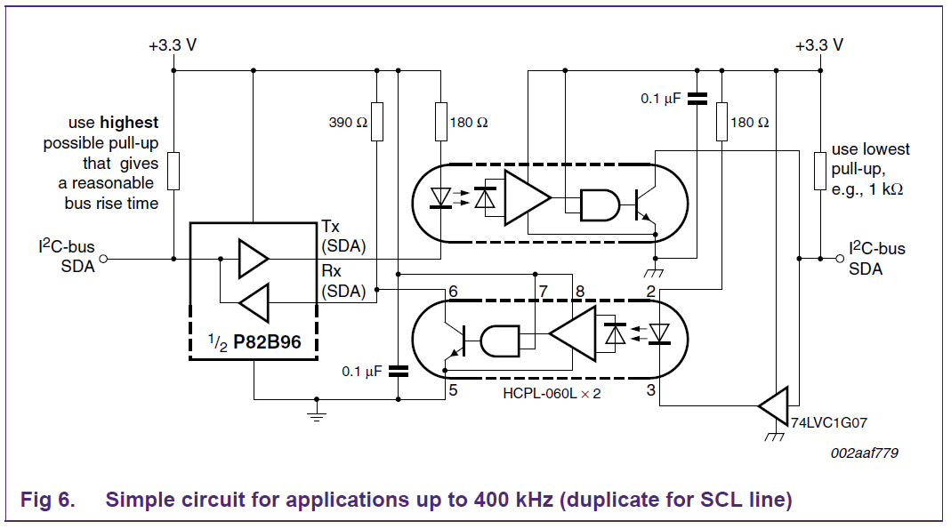
3.3V bias at 400 kHz:
It seems the simplest solution would be to go with this example. Does the fact that I'll operate the bus at 100 instead of 400 kHz affect the choice of values for the resistors on the optoisolator?
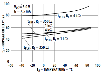
The datasheet for the opotisolator shown (HCPL-060L) includes this figure:

Which seems to indicate that a higher output resistor (\$ R_L \$) will result in longer propagation delay / lower frequency. Does that mean that a higher value would be a better choice for my application?
In short, which of these two examples is the best starting point, and what values do I need to consider changing?


