1
\$\begingroup\$

I'm newbie in PCB design and I'm trying to achieve my first 4 layer pcb.

Inner layers are gnd and vcc planes filled entirely with copper. My default trace/spacing is 0.1mm/0.1mm and drill size is 0.2mm.

I calculate that a via depending on that specs is limited to 0.5mA. Maybe I'm wrong. But if so, to transfer 2A from front layer to inner vcc plane, do I need to place at least 4 vias in front trace ?

What is the minimum clearance between this vcc via and inner ground plane ?

Thanks in advance for your help.

\$\endgroup\$
7
  • \$\begingroup\$ How did you calculate the via ampacity? Also, nothing prevents you using larger vias in a board with a minimum via size spec of 0.2 mm. \$\endgroup\$
    – The Photon
    Commented Feb 24, 2017 at 16:49
  • 2
    \$\begingroup\$ Even tiny vias can do a lot more than 500 uA! What diameter are your vias? \$\endgroup\$ Commented Feb 24, 2017 at 16:51
  • 1
    \$\begingroup\$ FWIW, the Saturn tool suggests 1.8 A limit for a 0.2 mm drill with 35 um plating. \$\endgroup\$
    – The Photon
    Commented Feb 24, 2017 at 16:53
  • \$\begingroup\$ I made a bad calculation !! But do I have to add at least 2 vias to get a 2A or more on vcc plane ? \$\endgroup\$
    – Alphapage
    Commented Feb 24, 2017 at 18:30
  • 1
    \$\begingroup\$ More vias = more current carrying capacity = better thermal conductivity. Any by the same measure, bigger vias = more current carrying capacity = better thermal conductivity. 0.1mm trace and space and 0.2mm drills is not your average PCB fab (and 0.2mm holes is borderline laser drilling), that's high-end stuff, and high-end = expensive. Just because that's the minimum that they can manage, doesn't mean you can't use 0.15 trace and space with 0.3mm drills (which is the most common rules for the vast majority of cheap-as Chinese board houses which are usually 10x cheaper than elsewhere). \$\endgroup\$
    – Sam
    Commented Feb 25, 2017 at 0:28

2 Answers 2

3
\$\begingroup\$

What is the minimum clearance between this vcc via and inner ground plane ?

This depends on the drill registration capability of your vendor, plus a bit of margin.

A typical figure at a shop capable of 0.1/0.1 space/trace and 0.2 mm drills is 0.25-0.3 mm for clearance from the hole to the plane (assuming no pad on the inner layers).

Another common way to deal with it is just include pads on the inner layers, and let the 0.1 mm copper-to-copper clearance, plus the pad annular ring, set the hole-to-plane clearance. Your fab shop might then ask to remove the inner layer pads to reduce drill wear, which I've always allowed them to do without issues.

\$\endgroup\$
1
  • \$\begingroup\$ I will increase clearance to 0.5mm because it is not a problem. \$\endgroup\$
    – Alphapage
    Commented Feb 24, 2017 at 18:28
1
\$\begingroup\$

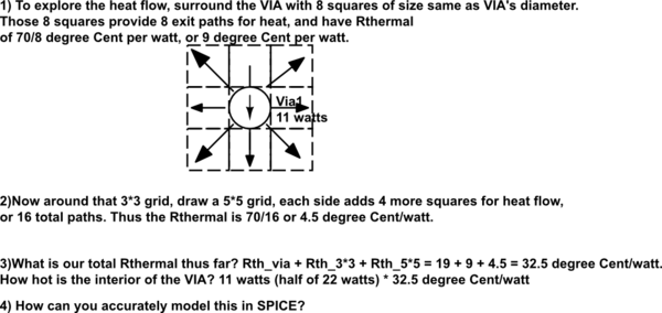
A useful starting point for via-design is the thermal resistance of standard copper foil: 1 ounce of copper per square foot is 1.4 mils or 35 microns thick. Given that thickness, the thermal resistance, from one edge of a square to the opposite edge with heat flowing laterally thru the foil, is 70 degrees Cent per watt. For any size square.

If your PCB house will plate the via to 35 micron thickness, and if the via circumference is the same as the via height, that ratio is 1:1 and you have a square of copper lining the inside of that drill hole. Thus we know its thermal resistance from top to bottom. Turns out, with heat able to exit in both directions, the thermal path drops by 2:1, and the heat flowing in each path is only 50% of the internally-generated via-heat, so Rthermal drops 4X to 19 degrees Centigrade per watt, IF THE VIA HAS 1:1 circumference/height ratio.

Are you willing to have the via operate at 225 degree Cent? Then you can have 225/19 == 22 watts dissipated inside that via.

An square of 1 ounce/foot^2 copper foil has electrical resistance of 0.000500 ohms, or 500 microOhms. With P=I^2*R, we have 22watts = II/2000, or I = sqrt(44,000) or I = 200 amps. wow.

This requires keeping the visible edges of the via at 25 degree Cent. Seymour Cray solved those problems with immersion into liquid coolants.


How cool can we maintain those vias? Here is a heat-flow diagram, looking down on the PCB:
schematic

simulate this circuit – Schematic created using CircuitLab

\$\endgroup\$
3
  • \$\begingroup\$ Sorry, I didn't understand anything, because I'm newbie and you are an expert. I think you already used such vias to vcc plane in hdi pcb maybe. It seems to be the new standard for such a pcb, but you are telling me it may require additional features to be able to achieve this. \$\endgroup\$
    – Alphapage
    Commented Feb 24, 2017 at 18:41
  • \$\begingroup\$ Can I bypass this thermal problem by increasing the number of vias ? \$\endgroup\$
    – Alphapage
    Commented Feb 24, 2017 at 19:36
  • \$\begingroup\$ Can I avoid or dodge this thermal problem? At 200 amps thru one via of ratio (circumference:height) of 1:1, there is 22 watts of heat you must handle, or the via continues to get hotter and hotter. Worse, copper resistance increases 0.4% per degree Centigrade. That is positive Feedback, tho not necessarily destructive. Can you remove 22 watts of heat? With large enough PCB area, directly connected to the VIA, a fan will adequately cool the VIA+Heat_Spreader. If you have enough PCB area. How much is needed? draw more squares around the via, as I've shown you. Investigate moving air cooling. \$\endgroup\$ Commented Feb 26, 2017 at 21:25

Your Answer

By clicking “Post Your Answer”, you agree to our terms of service and acknowledge you have read our privacy policy.

Not the answer you're looking for? Browse other questions tagged or ask your own question.