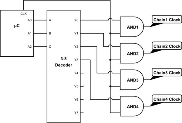
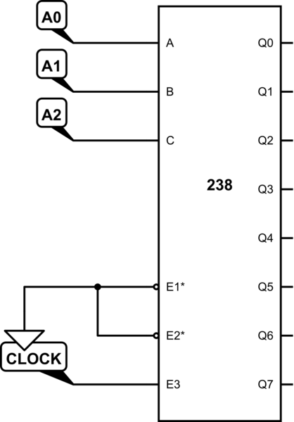
I'd like to route a single clock signal to one of several possible destinations by means of a few (2 or 3) address select lines.
Background: I'm driving 595 shift registers from a microcontroller (Arduino for now, possibly ESP8266 later). I want to have multiple (probably 4, possibly 5 or 6) separate chains of SRs that can be driven separately, so that I can (for example) drive 14 segment displays on each chain, and scroll (shift) each separately. My original design had all of the SR chains sharing \$\text{SER}\$, \$\text{RCLK}\$, and \$\text{SRCLK}\$ lines from the microcontroller, and using a 3-8 decoder to drive the \$\overline{\text{SRCLR}}\$ as a sort of "Chain select". However, I realized that \$\overline{\text{SRCLR}}\$ also clears the input registers, which would ruin the ability to scroll the outputs... I'd need to "refill" each SR chain after its \$\overline{\text{SRCLR}}\$ was low.
My next idea was to use a separate \$\text{SRCLK}\$ for each SR Chain. Option B of this ESE answer suggests the same approach. As long as \$\text{SRCLK}\$ doesn't change, any signals on \$\text{SER}\$ won't change the input registers and any change on \$\text{RCLK}\$ will re-latch the same data to output. However, I don't want to have multiple physical pins for the multiple clocks because (a) pin count constraints, and (b) I'll probably use the Hardware SPI port to send data to the SR chains.
Which leads me to the question. Assuming I have a single clock pin (output) from the microcontroller, how can I send that signal to only 1 of several possible destinations? Assume 3 address lines driving a 3-8 decoder, giving me 8 "SR Chain Select" signals. I'm considering using an AND gate for each SR Chain, with the clock as an input to each, and the 8 Chain Select signals as the other input to each (ignoring for now that most 3-8 decoders output 7 highs and 1 low, so I'll likely need an inverter on each decoder output line). See schematic below (only 4 AND gates shown for reduced size). Is this the best solution, or is there a better approach?

simulate this circuit – Schematic created using CircuitLab

