5
\$\begingroup\$

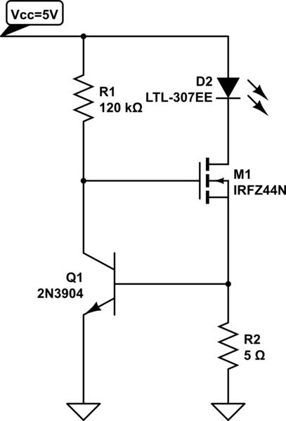
Here's a current limiter circuit that uses the negative feedback to limit the current to a certain point.
schematic

simulate this circuit – Schematic created using CircuitLab

I have not studied feedback systems before as I'm not an EE student just do it for fun. But here's what I know about this circuit:

When the current through R2 increases the voltage on the base-emitter would also increase. When the voltage reaches about 600mV Q1 will start to conduct. The collector current in Q1 will pull the gate voltage down due to R1 turning the mosfet off, hence reducing the current through the LED. Probably this will continue until Vbe and Vgs reach a certain set point.

Using the equation for a negative feedback loop, assuming the open loop voltage gain is G, we get for the closed-looped voltage gain

$$GV=\frac{G}{1+\beta G}$$ where the denominator takes account for the feedback fraction. Knowing all of this I want to calculate the Vbe and from that measure the current through the LED.

I know the open loop gain of the CE stage but don't know how to start off. I also don't know how to calculate the feedback fraction. I have not seen a practical example of such a circuit before. I want to go through each feedback loop and calculate everything, and finally get a good estimation for all circuit parameters. So any hint would be appreciated.

Here are some observations(out of breadboard):

For Vcc=5V and LED's FWD equal to 2V, I got the following readings:

Vbe=0.47V
Vgs=3.8V
I(led)=40-50mA

UPDATE 1:

I have written a simple code in matlab that runs through a loop for 5000 times, each time calculating a Vbe based on a new Ic. I used the fact that for a silicon NPN BJT the collector current is 4mA at Vbe=0.7V. For Is I took 8.11*10^-15A. I got a wide range of results as you see below. To save space I've kept some interesting ones. Here's the code and the output:

function clcm()

I=4E-3;
Vbe=0.7;
Ic=40E-6;
Is=8.11E-15;
Vt=26E-3;

R=zeros(10,3);

for i=1:5000
    Vbe=Vbe-Vt*log(I/Ic);
    I=Ic;
    Ic=Is*exp(Vbe/Vt);
    R(i,1)=i;R(i,2)=Vbe;R(i,3)=Ic;
end

disp(num2str(R))

end

Here's the output with the 2nd column indicating the Vbe and the 3rd showing corresponding Ic:

1     0.58026558  3.9954399e-05
2     0.58023592  3.9908849e-05
3     0.58020626  3.9863352e-05
4      0.5801766  3.9817906e-05
5     0.58014694  3.9772512e-05
6     0.58011729   3.972717e-05
7     0.58008763   3.968188e-05
8     0.58005797  3.9636641e-05
9     0.58002831  3.9591454e-05
10     0.57999865  3.9546318e-05

3630      0.4726373  6.3647499e-07
3631     0.47260765  6.3574938e-07
3632     0.47257799  6.3502461e-07
3633     0.47254833  6.3430065e-07
3634     0.47251867  6.3357753e-07
3635     0.47248901  6.3285523e-07
3636     0.47245936  6.3213375e-07
3637      0.4724297   6.314131e-07
3638     0.47240004  6.3069326e-07
3639     0.47237038  6.2997425e-07

4991     0.43227299   1.347568e-07
4992     0.43224334  1.3460317e-07
4993     0.43221368  1.3444972e-07
4994     0.43218402  1.3429644e-07
4995     0.43215436  1.3414334e-07
4996      0.4321247  1.3399041e-07
4997     0.43209505  1.3383766e-07
4998     0.43206539  1.3368508e-07
4999     0.43203573  1.3353267e-07
5000     0.43200607  1.3338044e-07

The Vbe=0.46V is what I exactly measured. I also measured collector current at about 6.8uA so it doesn't agree with what I got above. There should be some constraint that forces me to stop running the code up to a specific iteration, because it's giving me a broad range of currents and voltages. We know the system in a negative feedback should reach equilibrium somewhere.

UPDATE 2:

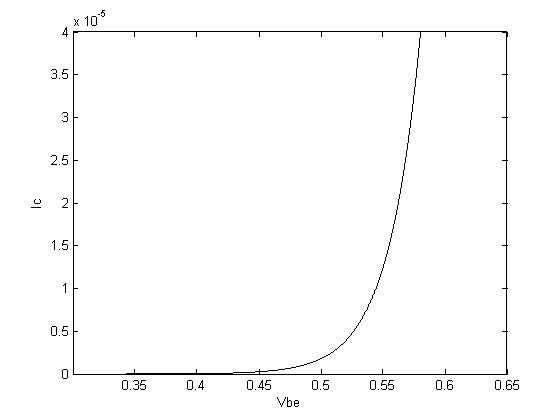
Here I have plotted the I-V characteristic of the BJT using the data I found above: enter image description here
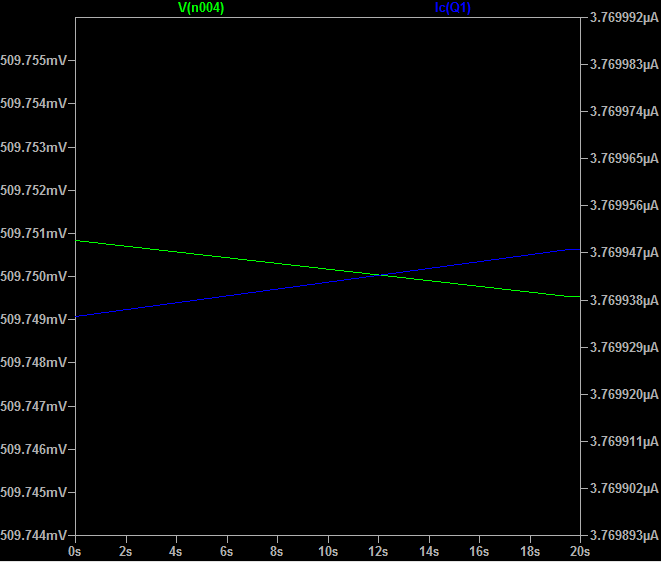
Here's the actual behavior of the circuit simulated in LTspice:

enter image description here

where V(n004) is the base-emitter voltage. As you see it doesn't agree with the above schematic. I'm actually trying to understand how I should modify the code to achieve the predicted result.

\$\endgroup\$
2
  • \$\begingroup\$ Until \$V_{be} \approx 0.65\:\mathrm V\$, Q1 isn't in its active region and this circuit won't be functioning as you'd expect. Try raising Vcc, though be aware that will put about \$0.65\:\mathrm V / 5\:\Omega = 130\:\mathrm{mA}\$ through the LED, enough to cook it unless it's more than a typical indicator LED. Increase R2 to 47Ω to get about 15mA. \$\endgroup\$
    – Phil Frost
    Commented Mar 18, 2017 at 19:19
  • \$\begingroup\$ I'll add a short note in my answer for the programming-minded, numerical-methods-enabled among us. \$\endgroup\$
    – jonk
    Commented Mar 18, 2017 at 21:54

3 Answers 3

3
\$\begingroup\$

To determine the loopgain properly you would need to make a small-signal equivalent of the circuit. The method of doing that will drag you straight into EE Analog circuit analysis territory. It's too complex to explain that all here so have a look here.

Since I know how to do this already I can tell you that in 1st order (omitting some 2nd order effects) the open loopgain is roughly:

$$G= gm * R1$$

Where

$$gm= 40 * I_{c,q1}$$

So we only need to know Ic,q1.

First determine the voltage across R1: 5V - Vgs,M1 - Vbe,q1 = 5 - 3.8 - 0.47 = 0.73 V

The current flowing through R1 is 0.73/120k ohm = 6.1 uA

The same current is flowing through Q1 so gm = 40 * 6.1 uA = 240 uA/V

So G = 240 uA/V * 120 kohm = 29

Maybe you wonder why the gain of NMOS M1 is not in this equation, it is because M1 is configured as a common drain or source follower. This means it has a voltage gain of about 1 so I neglected it. Only if M1 was a very small NMOS like an on-chip NMOS would it have such a small W/L that the gain would be significantly smaller than 1. But this is a switching NMOS and these have very large W/L to get the small Rds,on value needed for switching MOSFETs.

Also R2 does not come into the equation as the voltage across it is (in 1st order) set by M1, if R2 had a different value M1 would simply provide more or less current. Again this is a 1st order approach, if you'd calculate in more detail you would find R2 influencing the loopgain. In the 1st order approach, the value of R2 only determines the DC biasing current.

As an (on-chip) circuit designer I would not do this calculation for this type of circuit as it is a well-known "local feedback" construction with a clear dominant pole (at the gate of M1) and therefore it will always be stable and will simply work as long as you dimension it properly such that all the DC voltages in the circuit remain "sensible".

\$\endgroup\$
3
  • \$\begingroup\$ You just saved me a longer comment! hehe. \$\endgroup\$
    – jonk
    Commented Mar 17, 2017 at 22:12
  • \$\begingroup\$ @FakeMoustache I know about the small-signal analysis of transistors. I think I don't need to know about G because I assume beta*G is way greater than 1, so the close loop gain would be approximately 1/Beta. Now I just need to know what Beta is. \$\endgroup\$
    – dirac16
    Commented Mar 18, 2017 at 10:21
  • \$\begingroup\$ In for example an opamp + feedback circuit, G is the gain of the opamp and beta is the gain of the feedback. So in a 2x amplifier, example: calvin.edu/~svleest/circuitExamples/OpAmps/noninvertingAmp.gif the beta would be 1/2 (R1and R2 will have equal values). Your circuit does not have such a feedback circuit so we can assume beta to be 1 (one). \$\endgroup\$ Commented Mar 18, 2017 at 13:50
2
\$\begingroup\$

Since you write that you "just do it for fun," I'll take a different approach to finding quantities for the circuit.

A couple of things spring immediately to my mind. The first is the pattern of using a small-valued resistor together with a base-emitter \$V_{BE}\$ drop to set a current source/sink value. It's not at all unheard of for non-critical currents such as might be used with LEDs. The second thing was more a curiosity, which is the use of the MOSFET and wondering if it can work with a small enough gate-source voltage required by the supply rail in the circuit. It seems fine. But I had to check it out.

Then other things impinged. I noticed the relatively high value of \$R_1\$ (not in the sense of \$M_1\$'s gate capacitance, though that crossed my mind) but in the sense of setting/establishing the operating \$V_{BE}\$ of \$Q_1\$. That led me to further wonder about the likely actual \$V_{GS}\$ of \$M_1\$, because I'd want that when I looked things up in the datasheet for it (along with the likely drain current involved -- which would be on the other of perhaps a hundred milliamps, just glancing at it.)

Those things in mind, I mentally penciled out that I'd want \$Q_1\$'s \$V_{CE} \ge 1\:\textrm{V}\$ so that it stays in the active region and away from saturation (which would be bad, anyway, for \$M_1\$) but that it would probably have to be much higher in order to allow \$M_1\$ to do its job. So I called up this datasheet and immediately saw that \$\vert V_{GS}\vert\$ could be as bad as \$4\:\textrm{V}\$ with \$I_D\$ as little as \$250\:\mu\textrm{A}\$. That's not especially good news, but I then dropped down to the typical figures (1 and 2) and could see that they don't even specify a curve with \$V_{GS}\lt 4.5\:\textrm{V}\$. I'm not so sure I would have selected this device, given that.

But let's say it works. (It does, you say, and I believe you.) So I then popped over to this Fairchild datasheet, instead. They do go down to \$I_D=100\:\textrm{mA}\$ and suggest that a typical \$V_{GS}=3.2\:\textrm{V}\$. Given that and adding some margin, I would expect about one volt across \$R_1\$. This means \$I_C=\frac{1\:\textrm{V}}{120\:\textrm{k}\Omega}\approx 8\:\mu\textrm{A}\$. I know that I get about \$V_{BE}=700\:\textrm{mV}\$ with \$I_C=4\:\textrm{mA}\$ for \$Q_1\$, not uncommonly. So I can derate things so that I expect \$Q_1\$'s \$V_{BE}=700\:\textrm{mV}+26\:\textrm{mV}\:\cdot\:\operatorname{ln}\left(\frac{8\:\mu\textrm{A}}{4\:\textrm{mA}}\right)\approx 540\:\textrm{mV}\$.

That suggests about \$I_D=\frac{540\:\textrm{mV}}{5\:\Omega}=108\:\textrm{mA}\$. Assuming, of course, that \$M_1\$ will do that with such an "under-specification" for \$V_{GS}\$ for that \$I_D\$ current, which is 400 times as much as they guarantee when given \$V_{GS}=4\:\textrm{V}\$. So I don't know if I use that exact MOSFET in that toplogy.

The base-emitter junction voltage varies by as much as around \$-2.4\:\frac{\textrm{mV}}{^\circ C}\$ and so the controlled current may noticeably vary with temperature if there's enough change. Perhaps 1% for each \$2^\circ C\$. For LEDs, though, that is often fine.


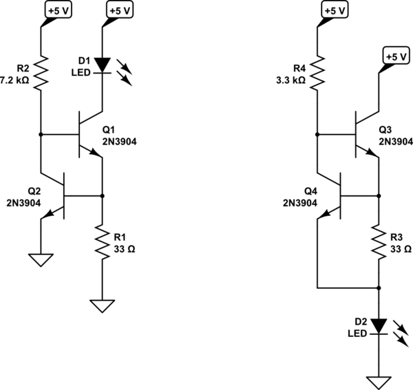
I like cheap BJTs. If I wanted to go the route you have laid out with two transistors (and assuming you only really want \$20\:\textrm{mA}\$ for the LED), I'd try something like this:

schematic

simulate this circuit – Schematic created using CircuitLab

Note that the NMOS is replaced by an NPN which doesn't require as much voltage headroom to operate. It does require some recombination current at the base, though. But quite tolerable, I think, and you can use most any BJT.

I started by first estimating the required base current for \$Q_1\$, which would be on the order of \$100-200\:\mu\textrm{A}\$. So I'd want to have at least that much for the collector current of \$Q_2\$. I selected \$500\:\mu\textrm{A}\$ total, both base drive for \$Q_2\$ and collector current for \$Q_1\$. I estimated \$V_{BE_1}=750\:\textrm{mV}\$ and \$V_{BE_2}=650\:\textrm{mV}\$, so \$V_{CE_2}=1.4\:\textrm{V}\$. This means \$R_2=\frac{5\:\textrm{V}-1.4\:\textrm{V}}{500\:\mu\textrm{A}}=7.2\:\textrm{k}\Omega\$. That's the left schematic. On the right, the LED takes away \$2\:\textrm{V}\$, so \$R_4=\frac{5\:\textrm{V}-1.4\:\textrm{V}-2\:\textrm{V}}{500\:\mu\textrm{A}}=3.6\:\textrm{k}\Omega\$. I picked a nearby value that was slightly lower.

The left side one is my preference of the two. It's sharper about holding the LED current stable, operates over a slightly wider range for \$V_{CC}\$, but does so at slightly higher cost in total current vs LED current.

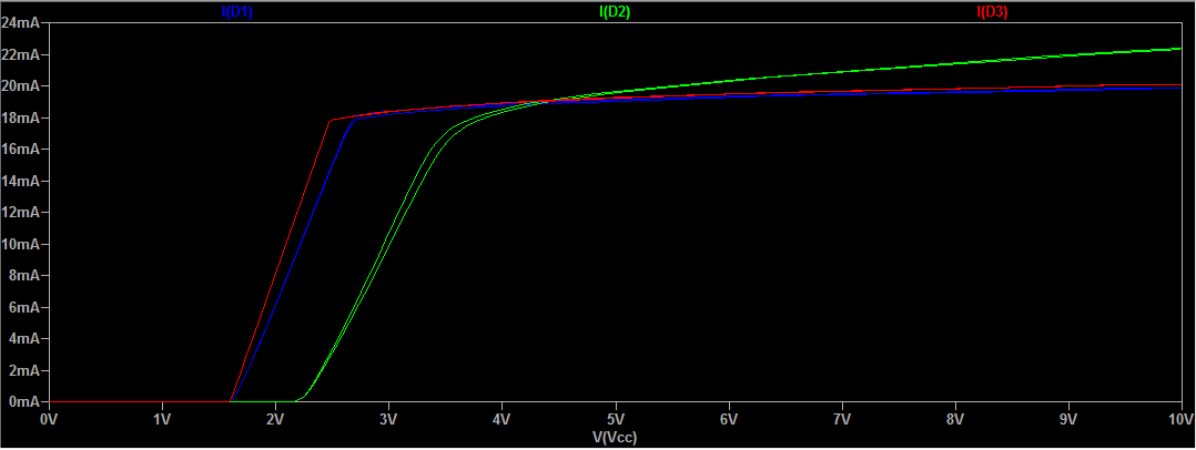
In case it helps, here's a spice plot that maps the differences in the three circuits. In the following picture, the x-axis is \$V_{CC}\$. (Nominally \$5\:\textrm{V}\$, but here allowed to span up to \$10\:\textrm{V}\$ so that you can see better how the LED currents stay relatively stable with variations in supply voltage.) The y-axis is the LED current. The red curve is for an NMOS version using a properly selected NMOS device for this lower voltage range. The blue curves are for the left hand schematic immediately above, with \$\beta\$ of both BJTs varied over a factor of 2. The green curves are for the right hand schematic immediately above, also with \$\beta\$ varying by a factor of 2.

enter image description here

You can see why some designers may prefer the NMOS approach. But you can also see why the left hand schematic may be nearly as good to some. And perhaps more readily available and cheaper. (I get my BJTs at 3 for a penny!)


NOTE: To set up a short programming loop to find the quiescent point, one might do the following, using VB.NET with the free community version of Visual Studio:

Sub Main()
    Dim R1 As Double = 120000.0
    Dim R2 As Double = 27.0
    Dim Vt As Double = 0.026
    Dim [is] As Double = 8.11E-15
    Dim k As Double = 0.005
    Dim Vth = 2.0
    Dim Vcc As Double = 5.0
    Dim Vc As Double = 3.0
    Dim Vb As Double
    Dim quadratic_b As Double
    Dim quadratic_c As Double
    Dim priorVc As Double
    Do
        priorVc = Vc
        Vb = Vt * Log((Vcc - Vc) / (R1 * [is]))
        quadratic_b = -2.0 * (Vb + Vth)
        quadratic_c = 2 * Vb * Vth + Vth * Vth + Vb * Vb - Vb / (R2 * k)
        Vc = (-quadratic_b + Sqrt(quadratic_b * quadratic_b - 4.0 * quadratic_c)) / 2.0
    Loop While Abs(Vc - priorVc) > Abs(0.000001 * Vc)
End Sub

In this case, the result I get is:

Vc = 4.48860154986336
Vb = 0.522075392320527
Ic = 4.26165375113863E-06
Id = 0.019336125641501

In the above code, I chose to model the active \$M_1\$ as a simple \$k\cdot\left(V_{GS}-V_{TH}\right)^2\$. You can see the value I used for \$V_{TH}\$ there, as well as for \$k\$. You can change those as you see fit, I suppose. The model for the BJT is about what you expect and I used your value for \$I_S\$. I also set \$\frac{k T}{q}=26\:\textrm{mV}\$.

The development is modest. Treating \$V_E=0\:\textrm{V}\$, I started out by initializing the value of \$V_C\$ to some middling value. The loop then computes the current through \$R_1\$ as \$I_C\$ and immediately computes the necessary \$V_B\$. An active mosfet has a set of differing rules, depending on what region it is in, but I just picked the simplest active mode as the only operating one. Or, in short, that \$I_D=k\cdot\left(V_{GS}-V_{TH}\right)^2\$. I also know that \$V_B=I_D\cdot R_2\$. Solving those two for \$V_C\$ led to a quadratic with \$a=1\$, which is left out of the above code. The other two terms are computed and then one of the solutions is chosen and applied to compute the next \$V_C\$. That's about all there is to it.

Just for kicks, I changed things up so that \$V_{TH}=1.5\:\textrm{V}\$ and re-ran it to get:

Vc = 4.03589373671807
Vb = 0.538560764992293
Ic = 8.03421886068278E-06
Id = 0.0199466949997146

The important result here is that \$I_D\$ didn't change much.

\$\endgroup\$
4
  • \$\begingroup\$ If you try R2=6 ohms what would you get for collector voltage? \$\endgroup\$
    – dirac16
    Commented Mar 19, 2017 at 10:41
  • \$\begingroup\$ @dirac16 I didn't plug in a full behavioral model for the NMOS -- mine completely ignores \$V_{DS}\$, for example, and seems to have an \$I_D\$ that only depends on \$V_{GS}\$ which of course is wrong. So the "mosfet" is grossly oversimplified in what I tossed together. I mostly was trying to point out that you need to include something where \$I_D\$ is a function of other factors. \$\endgroup\$
    – jonk
    Commented Mar 19, 2017 at 17:40
  • \$\begingroup\$ For R2=6 ohms I supposed the mosfet was in it's triode region. For that I chose the exact equation describing the mos in it's triode region but got strange values for Vc \$\endgroup\$
    – dirac16
    Commented Mar 19, 2017 at 17:57
  • \$\begingroup\$ @dirac16 Then if you want a crafted simulation the most important thing is that you can identify how the simulation will converge rather than diverge. What I intended to write only was supposed to work when the NPN and the NMOS are both known, a priori, to be in their active regions. You can assume just one quadrant of operation here, I suppose. But even there the NMOS has three different equations and the simple ones don't "blend" well to each other, either. If you approach this like spice, you will need to use the differentials. \$\endgroup\$
    – jonk
    Commented Mar 19, 2017 at 18:21
0
\$\begingroup\$

You don't need to calculate the current through the LED: you only need to calculate the current through R2. Since the current in the gate of M1 is effectively zero, R2 and the LED are in series and thus their current is equal.

Calculating the current through R2 (and thus, the LED) is easy because you know it's resistance, and you know Q1 is going to reach equilibrium around 0.65V so you know the voltage across R2 also. Ohm's law and you're done.

All you really need to know about the feedback is that the gain of Q1 is "high", which means feedback will keep the voltage across R2 "very close" to 0.65V unless the transistors can't operate in their active regions.

Of particular note in this circuit, you've chosen a MOSFET instead of a BJT for M1. MOSFETs typically have a threshold voltage higher than the analogous 0.65V threshold of a BJT. Be sure to select a MOSFET with a threshold voltage significantly less than 5V, otherwise M1 will never be able to turn on and you'll get no current at all.

That you've measured Vbe = 0.47V (not ~0.65V) tells me you are most likely having this problem. I bet if you swap out some different colored LEDs with different forward voltages (or even resistors), you'll find the current is not constant as you'd expect. With R2 = 5 ohms, LED current should be about 120mA. (Which I'd also note is too much for ordinary indicator LEDs: 15mA is a typical maximum.)

\$\endgroup\$

Your Answer

By clicking “Post Your Answer”, you agree to our terms of service and acknowledge you have read our privacy policy.

Not the answer you're looking for? Browse other questions tagged or ask your own question.