I completed a microcontroller project but I want to add a feature where when it starts up, it can read a 4-bit value defined by on-board jumpers (jumper closed = logic low, jumper open = logic high via microcontroller's internal resistor).
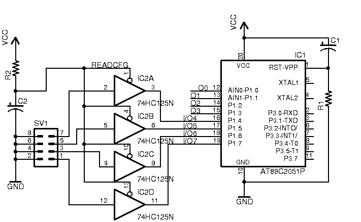
This is a circuit I came up with so far:
In reality I'm using an AT89S52 variant.
In any event, I ran out of usable GPIO pins and I do not want to sacrifice an existing feature just to read input at startup only once. In other words, the ideal solution to my problem is to connect the READCFG net to any GPIO pin directly but I'm out of free pins. (just ignore the unconnected pins in the diagram).
For the microcontroller reset circuit, I can get away with a simple RC network as shown to the right of my diagram, which causes the reset to take time which depends on the values of R and C.
Now I'm looking at using the same approach to read the configuration. Ideally, I want this to happen:
When a reset is issued to the micro controller, both RC networks reset (at least C1 will be shorted since the normal micro controller reset button will be connected to it).
Then on reset, the buffers (IC2) are immediately enabled so that jumper data (connections at part SV1) are recognized and loaded into 4 bits of the micro controller. In this example, the bits are loaded into P1.4 through P1.7. At the same time, the devices used as output that are connected to P1 are disabled via the appropriate value set from a GPIO pin of the micro. (for example, we can say P1 is connected to a simple 74HC573 latch with OE set to high).
I want the buffers (IC2) to be enabled for the same time as the micro controller reset period plus roughly 24 clock periods after that so that I can issue this command into the micro controller and then the inputs can be read:
mov A,P1 ;store contents of entire port into accumulator
Again, my main objective here is that when a reset is issued to the micro controller, the buffers (IC2) are enabled for as long as the reset plus at least enough time to completely process the "mov A,P1" instruction without using any extra IC's or requiring that READCFG be connected to a GPIO pin.
From my setup, what I do know is to make the time constant of C2/R2 higher than that of C1/R1 But I feel something else needs to be done to make my idea work. Could I somehow connect C2/R2 to the micro controller to produce a longer delay at READCFG net?
UPDATE
Based on the questions in a response, I'll answer them one by one.
- Why are you using latches and an RC timer to delay the assertion of your jumpers, wouldn't simply using pull-up resistors attached between the jumpers & your uC(uC=microcontroller), with the jumpers shorting back to ground, accomplish the same thing, without having to "wait to read" until the capacitor C2 charges?
This won't accomplish what I want because the P1 lines are used as input only at the beginning and then after, always as output until a reset happens. If I connected SV1 (jumper block) direct to the inputs of the micro, then as soon as I short a row of pins in the block, the micro and the output will be forced to receive a low value regardless of whether the micro needs to read from the block or send data to the output.
- If you're really intending to multiplex 4 I/O pins...
That sounds like the word I'm looking for except that 4 I/O pins are set to receive the jumper block data at the beginning then after a set time, all I/O pins only output data.
..., but you'll need a way to electrically isolate/disconnect your IC2 array from the I/O pins....
This is why I plan to use 74HC125. I believe the output of it is whatever the raw input is if the enable input is set to low. If enable input is high, then the output is set to high-impedance. But then wouldn't high-impedance value in all IC's be the same (100+Kohms)?
...after either 1: a predetermined timeout (such as using an RC timer, plus some MOSFETS {for example}) or 2: a signal sent from your mocrocontroller (call it a "read verified output") on another I/O pin to activate a similar disconnect circuit. Either would be feasible, but you'd have to tell us which you wanted in order for us to be able to help much there.
I want to issue the "disconnect" of the input block after a set RC timeout. The time must be at least the same amount of time it takes for the uC to reset plus the time it takes for the microcontroller to fully execute the "mov A,P1" instruction.
- Is there a specific reason why you're wanting to avoid adding any "additional ICs" to your circuit.
Board real-estate, costs, practicability, and routability. I have a circuit board that doesn't have much room and adding an IC requires more routing and space the costs go up if I require more board and its more practical for me if I can do the timing with just an RC network instead of doing a full-blown timeout solution with an IC.
... (By my count, you're already proposing adding 4 ICs in the form of latches)?
Actually, the latches for output will be contained in 1 IC. The output situation is fine. the input situation is what I need help with. The buffers (74HC125) are 4 buffers inside a single 14-pin IC.
Or would adding 1 serializer (aka shift register) to read all 4 jumpers into a single I/O pin possibly be the least complicated, and most readily achievable solution here?
That could make things more intense in software and hardware. I'll then need to implement timing of some sorts to shift the bits out and read them one at a time in the micro. On top of that, I'll have to latch the input data somehow as well. I can't go with this idea because it will require more circuitry to process properly and also I'll have to activate the internal shift register latch to load in the data. I'm better off with my idea because then I get to skip shifting bits one-by-one.


