1
\$\begingroup\$

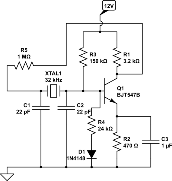
I am trying to built an oscillator at low frequeny (32768 Hz). After some research i have chosen to build a pierce oscillator. Here is my schematics : discard
schematic

simulate this circuit – Schematic created using CircuitLab

I have tested the amplifier with a function generator producing 32Khz and it worked well, i have observed a gain of approximatively 3.7. The load capacitance of the cristal is about 12.5pF. I am not seeing any oscillation at the collector. Any idea about what could be wrong in my setup ?

Thanks !

\$\endgroup\$
2
  • \$\begingroup\$ Your diagram appears wrong. Hopefully this is not the same as your circuit. | The xtal is short circuited by a wire. Presumably the LH end of xtal should connect to Q1 collector. | R1 = 3.2 Ohm - should that be 3.2 k Ohm??? | Gain is approx R1 / (R2 + 26/Ic_ma) . For R1 = 3K2 gain is ~~~ 7. | Vb~= 1.7V. So Ie ~= (1.7-0.6)/470 ~= 2 mA. VR1 = VR2 x R1/R2 = 1.1 x 3k2/470r = 7.5V. Vce ~+ 12-1.1-7.5 = 3.4V so transistor is not hard on (which is good) \$\endgroup\$
    – Russell McMahon
    Commented Apr 13, 2017 at 15:17
  • \$\begingroup\$ Oh yes my bad, that the first i use the schematics editor, the LH of the xtal is connected to the collector. Yes R1 is 3.2K. Thanks a lot @Russel : I have carrefully designed the amplifier part (that the first timefor me ^^) \$\endgroup\$
    – Nicolas
    Commented Apr 13, 2017 at 15:28

2 Answers 2

1
\$\begingroup\$

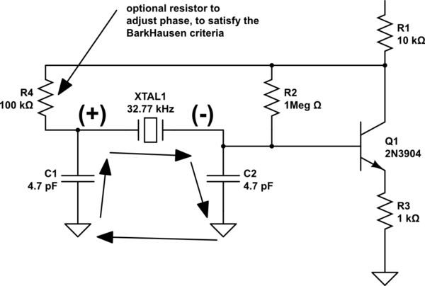
The crystal + 2 caps form a PI network:

schematic

simulate this circuit – Schematic created using CircuitLab

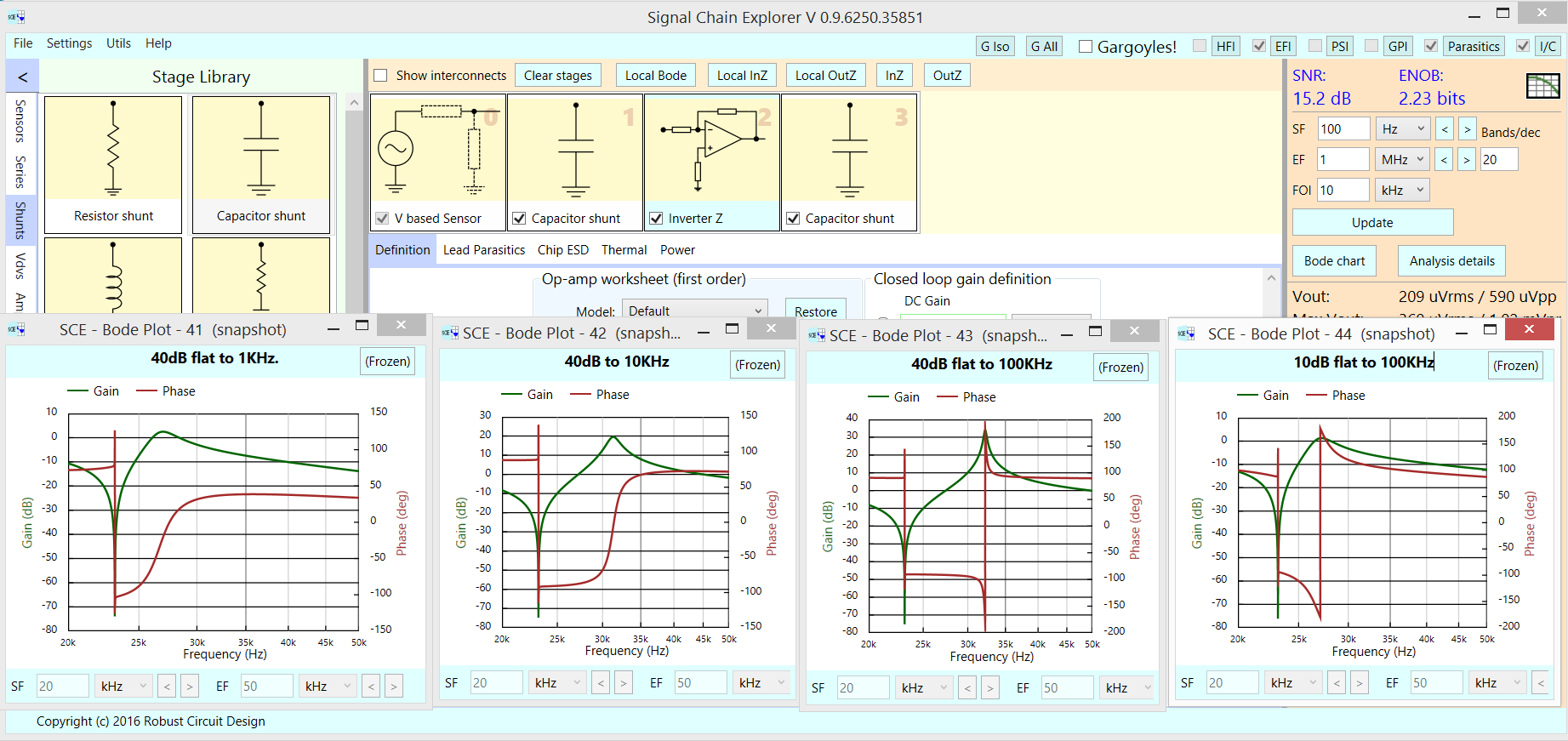
Lets examine the loop gain and loop phaseshift; here in Signal Chain Explorer, the XTAL model is embedded as Z(feedback) of the Inverting OpAmp stage; crystal inductance is 58.9766 Henry; capacitance series/resonance is 0.8pf; the plate-to-plate capacitance is also 0.8pF; Rloss is 1Kohm.

I reduced the two capacitors of the PI network, here before and after the OpAmp, from 22pF to 4.7pF. I've read the low frequency oscillators need small capacitors, so the energy is not shorted to GND.

Key point is the gain and bandwidth of the OpAmp. With gain of 10dB (3.16x), shown in the far right BODE, the gain is barely above 0dB.

In contrast, examine the 40dB gain, flat to 100KHz, and see a healthy peak (30+dB gain) at the correct frequency.

Does the value of R4 (in the schematic) matter? Lets examine that next.

enter image description here

\$\endgroup\$
2
  • \$\begingroup\$ Nice! Can you send me your simulation? Question : are they the bode diagrams for the closed loop ? What is the parameter whose value is changing for the three first left diagrams ? \$\endgroup\$
    – Nicolas
    Commented Apr 14, 2017 at 9:31
  • \$\begingroup\$ @ Nicolas The changing param is the UnityGain Bandwidth of the opamp. Leftmost sim has 40dB gain, with rolloff at 1KHz (for a 32KHz oscillagtor). Left-1 sim has 40dB gain, rolloff at 10KHz (for a 32KHz oscillator). Left-2 sim (which shows the snappy phase changes, desirable for accurate oscillation) has 40dB gain, rolloff at 100KHz. \$\endgroup\$ Commented Jul 3, 2018 at 3:26
0
\$\begingroup\$

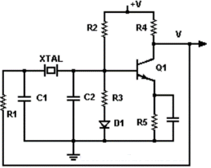
This is not a Pierce oscillator because there is no feedback. A typical scheme, where R1 is feedback:

enter image description here

\$\endgroup\$
10
  • \$\begingroup\$ The wire from lh end of crystal on his diagram should go to collector. The cct is then similar to yours. His R1 is vastly too low - which may be a typo. \$\endgroup\$
    – Russell McMahon
    Commented Apr 13, 2017 at 15:19
  • \$\begingroup\$ How do i choose the value of R1 of the above diagram ? 1MOhm ? \$\endgroup\$
    – Nicolas
    Commented Apr 13, 2017 at 15:28
  • \$\begingroup\$ R1 and C1 provide a phase delay of 65 °(link) to the feedback signal. \$\endgroup\$
    – AltAir
    Commented Apr 13, 2017 at 15:47
  • \$\begingroup\$ Another example link. With a value of components. \$\endgroup\$
    – AltAir
    Commented Apr 13, 2017 at 16:00
  • \$\begingroup\$ @RussellMcMahon Actually, OPs R4 was too low (though he fixed that in edit), his R1 is still entirely nonexistant (straight trace from XTAL to collector, no resistor) \$\endgroup\$ Commented Apr 13, 2017 at 16:33

Your Answer

By clicking “Post Your Answer”, you agree to our terms of service and acknowledge you have read our privacy policy.

Not the answer you're looking for? Browse other questions tagged or ask your own question.