0
\$\begingroup\$

I am using the U62256A 32K x 8 bit static RAM. For testing purposes I connected all outputs to LEDs and since they are also inputs to a dip-switch so I'm able to write data.

The write mode works nicely and stores everything correctly. Data rentention in the RAM chip is also working. What doesn't quite work to my satisfaction is the read mode. Stored 1's (high) are properly output at a stable 5V, but 0's are flickering. My cheap voltmeter reads about 2.4V at the output and the LEDs are visually flickering at about half the brightness of a high output. According to the datasheet there should be a maximum voltage of 0.4V when the output is low.
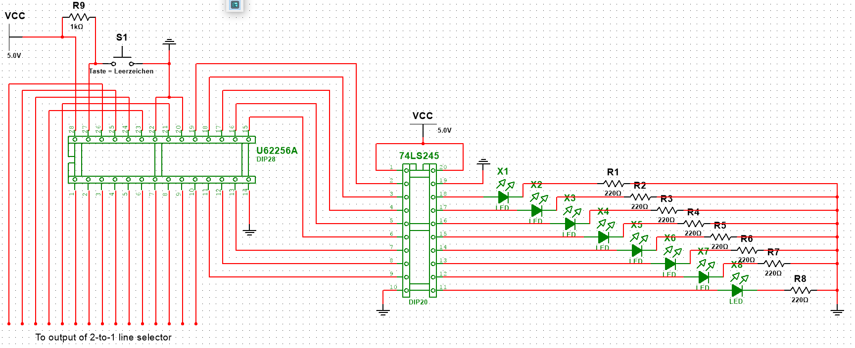
my circuit This is the circuit. The right side of the LS245 is there so I can connect the RAM output to a bus. I have already tried removing it and connecting the outputs directly to the LEDs, as well as disconnecting the dip-switches (not shown in the schematic). I'd like for the LEDs to be simply off when the outputs are low, but with my little knowledge on electronics I can't figure out why they are flickering or what to do about it.

I'll appreciate any and all help!

\$\endgroup\$
4
  • \$\begingroup\$ If you disconnect the LEDs do you read the expected voltages? \$\endgroup\$ Commented Apr 19, 2017 at 1:18
  • \$\begingroup\$ Your schematic would be much more useful if you showed the pin names (A0, A1,.. , D0, D1..., etc.). The ~W write enable requires a pull-down resistor to ensure that it will go low when you press the button. What are you doing with the address and data lines? They must be held in known states by tying to Vcc or Gnd, or with pull-up or pull-down resistors. If the inputs are not held in a known stare, they will wander randomly between High and Low. \$\endgroup\$ Commented Apr 19, 2017 at 2:09
  • \$\begingroup\$ The address inputs are connected to the output of a 2-to-1 line selector so I can choose between an address from a register or manual input. The write enable pin is pulled up. I just updated the schematic. Unfortunately I don't know how to change the pin names in the program I'm using. \$\endgroup\$
    – padarom
    Commented Apr 19, 2017 at 8:34
  • \$\begingroup\$ A voltage of 2.4V implies that you have a bus conflict, something is pulling the wire high at the same time as the SRAM is trying to pull it low. What is the voltage on the lines when the SRAM read line is idle? When idle pull the data line high and then low using a 1k resistor, if it doesn't go to both rails then something else is driving those pins. \$\endgroup\$
    – Andrew
    Commented Apr 19, 2017 at 8:39

2 Answers 2

1
\$\begingroup\$

The fact that you have tied the \$\overline G\$ and \$\overline E\$ pins hard to ground is probably your issue.

Both those pins are edge triggered to perform control of the outputs.

WORSE: With them both tied that way, when you try to write to the device you will need to overdrive the outputs of the device. This will probably damage the internal line drivers.

You should read the specification carefully, and apply appropriate timing to ensure you are supplying edges and levels at the correct times and never back driving the device.

\$\endgroup\$
4
  • \$\begingroup\$ From how I understand the datasheet this shouldn't be an issue as the timing diagram specifies the read mode is finished on the falling edge of \$\overline W\$ before writing to the device. Data retention is also only possible while the \$\overline E\$ pin is low and there is no situation I can see in my application where I want to disable the chip, so I can't see why \$\overline E\$ is an issue? \$\endgroup\$
    – padarom
    Commented Apr 19, 2017 at 13:14
  • \$\begingroup\$ @Padarom since you are using only \$W\$ the outputs do not turn off till you drop it, and return to outputs when you raise it. However he data is clocked in when you raise \$W\$ so obviously you still need to be driving the data lines at that point. Since \$t_{LZWE}\$ is minimum zero, that means a collision on the bus. \$\endgroup\$
    – Trevor_G
    Commented Apr 19, 2017 at 13:24
  • \$\begingroup\$ You may get away with just using \$G\$ properly and tieing \$\endgroup\$
    – Trevor_G
    Commented Apr 19, 2017 at 13:25
  • \$\begingroup\$ This is not an answer to the question why the LEDs are flickering. \$\endgroup\$ Commented Oct 10, 2019 at 6:59
0
\$\begingroup\$

The LED's are flickering because:

  1. I see no bypass capacitors on the 5 volts lines, specifically at the power and ground pins to each and all IC's. This can make LED's flicker but also make IC's not behave correctly. Use 100nF caps at each IC and a 100uF cap for LF transients due to LED's changing state.

  2. The 74LS245 needs to be a 74LS374 latch so that the RAM can change outputs first, then a simple rising-edge pulse to the CLK pin of the 74LS374 will update the LED's with no flicker. Using a 74LS245 buffer outputs the flicker from the RAM, which is due to it changing states at the output.

  3. Updating RAM or the RAM address and updating the LED's MUST be 2 separate events, even if only microseconds apart.

\$\endgroup\$

Your Answer

By clicking “Post Your Answer”, you agree to our terms of service and acknowledge you have read our privacy policy.

Not the answer you're looking for? Browse other questions tagged or ask your own question.