0
\$\begingroup\$

I posted this circuit in a question about protection clamping, but got a lot of questions around the circuit itself.

Is this not a good / the normal way to shift and amplify a low amplitude (75mv) swinging around ground signal (simulated by Vin) to Vout: 2.5V amplitude signal swinging around ca 2.5V (2.79) ?

For the sake of simplicity Vbat is a stable, regulated 12v source.

Vin is a current sensor, so Vin is practically a DC signal.

The implementation of the circuit gave me a lower than expected center (ca 1.8v) I guess that can explained by too low bias current?
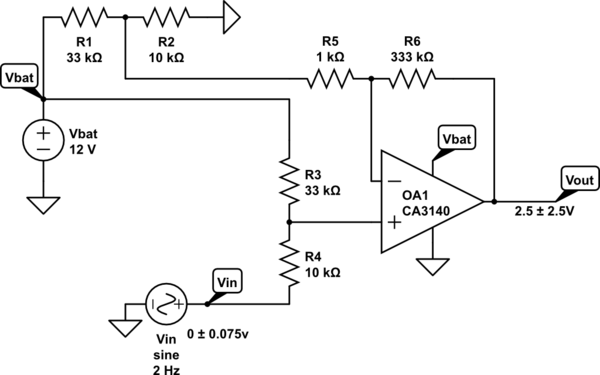
schematic

simulate this circuit – Schematic created using CircuitLab

\$\endgroup\$
4
  • \$\begingroup\$ What gain did you compute for that? Did you ground your VIN when measuring your VOUT? Have you looked at the input offset voltage for the CA3140?? \$\endgroup\$
    – jonk
    Commented Jun 9, 2017 at 18:28
  • \$\begingroup\$ If you suppress Vin and connect R4 directly to ground, Vout is ? \$\endgroup\$ Commented Jun 9, 2017 at 19:13
  • \$\begingroup\$ The gain resistors are trial and error in simulator to get 75mv = 5V(2.5), so I guess that's a gain of 33, and yes, I grounded Vin when reading the center. offset voltage should be 5 / 15 mV according to datasheet. Resistors are 1%. \$\endgroup\$
    – ttyridal
    Commented Jun 9, 2017 at 19:14
  • \$\begingroup\$ Ok. I get a gain of about 29.55, given your resistor values and assuming perfect values. \$R_{TH}=\frac{R_1\cdot R_2}{R_1+R_2}, V_{TH}=V_{BAT}\cdot\frac{R_2}{R_1+R_2}, V_-=\frac{V_{OUT}\cdot \left(R_5+R_{TH}\right)+V_{TH}\cdot R_6}{R_5+R_6}, V_+=\frac{V_{IN}\cdot R_3+V_{BAT}\cdot R_4}{R_3+R_4}\$ and solving \$V_-=V_+\$ to get \$\frac{\textrm{d} V_{OUT}}{\textrm{d} V_{IN}}\$. But I also now understand your question about the output voltage. It's not right. \$\endgroup\$
    – jonk
    Commented Jun 9, 2017 at 19:35

1 Answer 1

1
\$\begingroup\$

I would prefer to shift the voltage with a parallel power supply. Something that resembles a zener, a shunt voltage reference. Look at something like this: http://www.ti.com/lit/ds/symlink/lm4040-n-q1.pdf

This would provide a very stable 2.5v reference. That means you don't need R1, R2 R3 and R4, eliminating errors and variance.

But anyway. If you're just trying to measure a shunt your best bet is to use an IC designed for that and you can save money and time. Take a look at this, and search for one that is better suited: http://www.ti.com/lit/ds/symlink/ina180.pdf

http://www.ti.com/lit/ds/symlink/ina301.pdf

Specially the INA180 will already give you an output at half the supply voltage. You just need to connect both inputs at your measuring resistor and you're done. Errors due to offset voltage and current will be reduced with the specifically-designed IC.

Hope it helps

\$\endgroup\$
3
  • \$\begingroup\$ Yeah. I've actually done a second design with ina199 after suggestions in another answer here on se. At this point this is purely academical to improve my op amp understanding. Would I not still need R3 and R4 for the voltage adder / summing? \$\endgroup\$
    – ttyridal
    Commented Jun 9, 2017 at 19:03
  • \$\begingroup\$ If the shunt needs to be grounded you could replace R4 with a zener and then you'd have Vin+2.5V at tha V+ input. \$\endgroup\$
    – Andrés
    Commented Jun 9, 2017 at 19:20
  • \$\begingroup\$ I'm not sure I understand how I should implement what you're suggesting. May I ask for an illustration? I can't really do anything with the shunt. It's connected between negative battery terminal and the load. my circuit has ground at the negative terminal. \$\endgroup\$
    – ttyridal
    Commented Jun 9, 2017 at 20:08

Your Answer

By clicking “Post Your Answer”, you agree to our terms of service and acknowledge you have read our privacy policy.

Not the answer you're looking for? Browse other questions tagged or ask your own question.