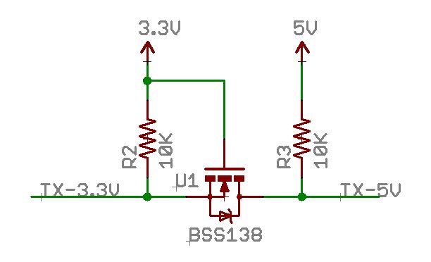
Here's quite a simple one and it is bi-directional too: -

When the data input from the 3.3 volt side is low, U1 turns on and connects the right hand data pin to the input data pin hence the output is also 0 volts. When the input pin is high, the transistor is turned off and the output on the right is pulled up to 5 volts.
Only thing to watch out for is speed of data - the rise time on the output 5 volt side is limited a little bit in reaching 5 volts from 3.3 volts. The first 3.3 volts is OK because the capacitance of the MOSFET couples the rising 3.3 volt data input signal to the output but, once the input side has settled at 3.3 volts, the remaining 1.7 volts are only attained via R3 charging up the internal parasitic capacitance of the BSS138 (about 20 pF including reverse transfer capacitance). RC time is therefore 200 ns which will be good for data rates up to 1 or 2 Mbps.
If you think you need faster then you can lower R3 maybe to 1 kohm. Then the only limiting factor is the specified rise and fall times of the MOSFET itself and these are maximums of 18 and 14 ns respectively but, watch out for the turn-off delay time - it is 36 ns compared to 5 ns for turn on-time. The effect of this will be to slightly alter the mark-space ratio of your data. It could be a problem but I suspect not at 2 Mbps if you lower R3 to 1 kohm.


