0
\$\begingroup\$

I'm sending two complementary PWM signals from a control board to a separate power board via a ribbon cable (along with some other signals, 20cm or so). The PWM signals control a MOSFET driver on the power board which, in turn, switch two MOSFETs as part of a half-bridge. I've noticed that as soon as I plug in the PWM signal there's up to ~100mV of noise on the 3.3V rail of the control board (checked with a scope). Since I'm using the 3.3V as a reference for ADC on the control board this is leading to substantial error in the ADC readings.

Is the wiring itself responsible for much of this noise? Wondering if this design is even feasible and whether it would make much difference to move the MCU, etc. from the control board to the power board in order to avoid wiring.

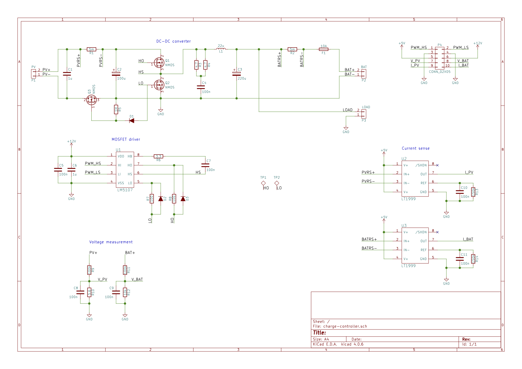
Schematic of the power board: power board schematic

\$\endgroup\$
8
  • 1
    \$\begingroup\$ Show us an schematic. \$\endgroup\$ Commented Jul 5, 2017 at 13:56
  • \$\begingroup\$ Added a link to the power board in the text above. I don't have a schematic yet for the control board. It's just voltage regulators and an STM32F103C8 "blue pill" board. Will eventually lay out a real PCB for this if I can get things working well. \$\endgroup\$
    – scttnlsn
    Commented Jul 5, 2017 at 14:02
  • \$\begingroup\$ The schematic looks unreadable to me (low resolution). Also, don't just link it, show it explicitly in your question. \$\endgroup\$ Commented Jul 5, 2017 at 14:10
  • \$\begingroup\$ OK, attached the image directly to the question \$\endgroup\$
    – scttnlsn
    Commented Jul 5, 2017 at 14:13
  • \$\begingroup\$ Now use the in-built schematic editor to draw your control board. Otherwise, we don't have enough information to help. \$\endgroup\$ Commented Jul 5, 2017 at 14:22

2 Answers 2

1
\$\begingroup\$

You are most likely experiencing the effects of current in the return path of your switcher. You can easily check this by measuring the ground with your scope on the ADC ground and on the ground near your sense circuits on the power board (without moving the scope ground). You will likely see the same 100 mV noise between the grounds.

When mixing power with signal, you will have keep in mind that the current return paths back to the battery and the load are not at the same instantaneous voltage at various points along the paths, due to the inductance and the resistance of the path. The paths for signal voltage references should be separate, connected at a single point, and should not have any current (don't share paths or use a ground plane that carries current). If you do have a ground plane, keep your reference signal path separated from it; even if it is on another layer, if you run a signal over a current-carrying ground plane, you can capacitively couple the switching noise.

Hope this helps.

\$\endgroup\$
2
  • \$\begingroup\$ Thanks. I will try that measurement later when I get a chance. The power board has a high current path with its own ground plane and a separate portion of the board that contains the MOSFET driver and current sense amps. The two ground planes on the power board are only connected by ~1cm wide bit of copper but perhaps this should be a much smaller trace? \$\endgroup\$
    – scttnlsn
    Commented Jul 5, 2017 at 16:15
  • \$\begingroup\$ I should also say, I see the noise even when there's no current through the FETs. I can disconnect the PV, BAT and LOAD and still see the switching noise. \$\endgroup\$
    – scttnlsn
    Commented Jul 5, 2017 at 16:21
0
\$\begingroup\$

Yes - switching noise is coupling into your vcc/ground. Try connecting wires adjacent to your PWM signal to ground (ie. GND-PWM1-PWM2-GND) - grounds will aid in shielding other signals from PWM (at least it worked for Parallel-ATA)

\$\endgroup\$

Your Answer

By clicking “Post Your Answer”, you agree to our terms of service and acknowledge you have read our privacy policy.

Not the answer you're looking for? Browse other questions tagged or ask your own question.