1
\$\begingroup\$

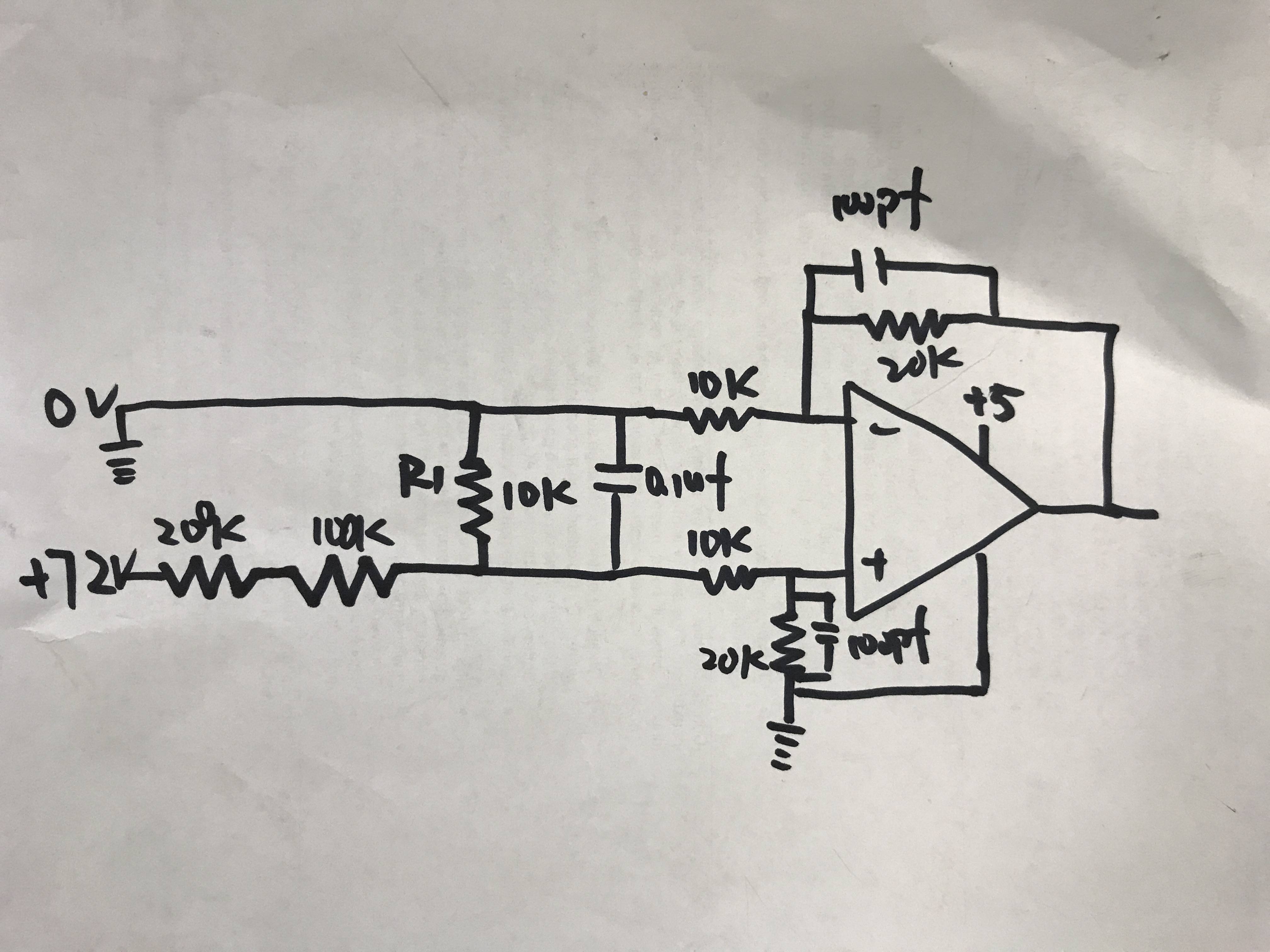
Schematic 1

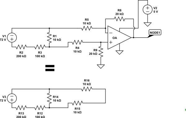
I'm using above 1:2 differential opamp, when 72V applied to the 30:1 voltage divider, voltage across R1 is only 1.727V instead of 2.4V, opamp output is around 3.4V.

Opamp is LMC6062IN/NOPB http://www.ti.com/lit/ds/symlink/lmc6062.pdf

I think it's because of bias current, any suggestion on solution?

Follow up question:

Same circuit below but now this time 0V does not connect to circuit main GND, so there is not second voltage divider but i am seeing around 1.5V across R1
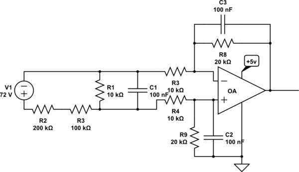
schematic

simulate this circuit – Schematic created using CircuitLab

Follow up question #2:
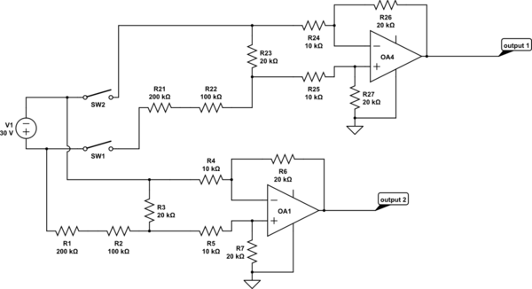
schematic

simulate this circuit

Switch on both side of V1, top and bottom circuits are identical differential opamp circuit, bottom one is before switches and connect to v1 directly, top one is after two switches.

When SW2 is open, SW1 is closed: voltage across R3 is 1.4v, output 2 is 2.83v. voltage across R23 is 0.532v, output 1 is 1.08v. Seems like R3 is in parallel with a 60K resistor, does that mean two op amps' inverting and non-inverting pin are tied together? I am using a dual op-amp.

\$\endgroup\$
7
  • \$\begingroup\$ Opamp bias current varies by many orders of magnitude depending upon which part it is. Usually the current is such to pull the voltage higher as well - you need to give us more information - especially the part number! \$\endgroup\$ Commented Jul 20, 2017 at 18:25
  • \$\begingroup\$ Part number is LMC6062IN/NOPB \$\endgroup\$
    – yxing
    Commented Jul 20, 2017 at 18:26
  • \$\begingroup\$ What are the two resistors on the left? 200k and 100k? There's a schematic button on the editor toolbar. It's very easy to use and much better than markers. \$\endgroup\$
    – Transistor
    Commented Jul 20, 2017 at 18:31
  • 3
    \$\begingroup\$ Have you considered the effect of the 10k and 20k resistors to the right of R1 (10k) in terms of the voltage divider, or are you just ignoring them? \$\endgroup\$ Commented Jul 20, 2017 at 18:35
  • 1
    \$\begingroup\$ Note: Please provide designators for all the components in your circuit so we can talk about R2 and R3 instead of "the resistor near the noninverting input". \$\endgroup\$
    – The Photon
    Commented Jul 20, 2017 at 18:38

3 Answers 3

5
\$\begingroup\$

... when 72v applied to the 30:1 voltage divider ...

It's not 30:1, it's 31:1. \$ V_{OUT} = V_{IN} \frac {10k}{200k + 100k + 10k} \$.

... voltage across R1 is only 1.727 V instead of 2.4 V.

But you have a second voltage divider in parallel with R1. "R1" is now effectively 7.5 kΩ. The voltage at R1 will be \$ V_{OUT} = V_{IN} \frac {7.5k}{200k + 100k + 7.5k} = 72 \times 2.44\% = 1.75 \; V\$ and the voltage into the non-inverting input will be 2/3 of that = 1.17 V.

Im (sic) thinking its because of bias current ...

I'm thinking it's because of biased thinking ...


schematic

simulate this circuit – Schematic created using CircuitLab

Figure 1. OP's second attempt.

In the standard inverting and non-inverting op-amp amplifier configurations the output will adjust until the difference between the two inputs is very close to zero. For practical analysis they are connected together as shown in Figure 1. Now it is clear that you have 20k in parallel with your 10k of R1 giving 6.67k.

Running the calculation again the voltage at R1 will be \$ V_{OUT} = V_{IN} \frac {6.67k}{200k + 100k + 6.67k} = 72 \times 2.17\% = 1.56 \; V\$


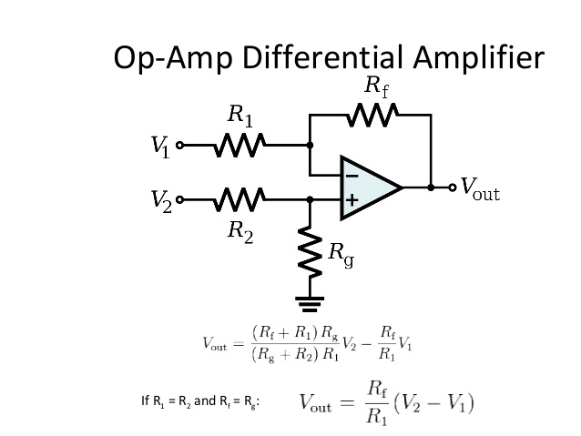
Your question 2 circuit is a bit of a mess and I don't think I could analyse it for you. I think you are trying to combine a traditional voltage divider on an non-ground referenced source and feed this into a differential amplifier. I doubt that this is necessary.

enter image description here

Figure 2. Just use the differential amplifier itself.

For example, setting R1 and R2 to 100k and Rf and Rg to 1k would give you a differential amplifier with a gain of 1/100. Your 72 V input on the original circuit would then give an op-amp output of 0.72 V (if it can swing that low).

Why complicate things?

\$\endgroup\$
9
  • \$\begingroup\$ Thanks for your explanation, what if I disconnect 0V from GND? \$\endgroup\$
    – yxing
    Commented Jul 20, 2017 at 20:11
  • \$\begingroup\$ Please state clearly what you are asking. Disconnect what 0 V from what GND? Do you mean disconnect the link between your circuit GND (0 V) and mains ground? What do you expect / want to happen? Are you hoping this will fix your divider error? \$\endgroup\$
    – Transistor
    Commented Jul 20, 2017 at 20:13
  • \$\begingroup\$ Yes I mean break the connection between 0v and main GND (two separate power supply), if so there will be no second voltage divider but I am still not seeing 2.32v across R1. \$\endgroup\$
    – yxing
    Commented Jul 20, 2017 at 20:24
  • \$\begingroup\$ Edit your question and add a schematic of your new setup including power supplies. Leave the old one there or all the answers will look ridiculous. As others have said, number your components. Add link to datasheet so we don't have to search for it. \$\endgroup\$
    – Transistor
    Commented Jul 20, 2017 at 20:27
  • \$\begingroup\$ just edited it. \$\endgroup\$
    – yxing
    Commented Jul 20, 2017 at 20:43
4
\$\begingroup\$

Another problem you may run into with your circuit is the input common mode range of the opamp.

For this device the input must not go closer to the positive supply rail than 2.6v to guarantee correct operation. If the supply rail is 5v this is equivalent to 2.4v relative to ground - if your supply rail is slightly low (it won't be exactly 5v) the max voltage may be lower. A typical device will work better up to about 3v.

From the calculations done by @Transistor you do have margin but it is something to be aware of.

There are a number of devices with improved input common mode range - often referred to as "Rail-to-Rail inputs" - I quite like the LMP7701 range that have very good offset voltage, extremely low bias current and can operate with a supply up to 12v.

Common Mode Range

\$\endgroup\$
1
\$\begingroup\$

This is a classic mistake, as you are assuming that your difference amplifier circuit is acting as a high impedance load to your signal source and front end circuitry. It doesn't, there is a (relatively) low impedance path through R4 and R9, as well as through R3 and R8. This is similar to how non-inverting amplifier circuits (such as simple voltage followers) act as high-impedance buffers, but inverting amplifiers do not. Transistor already did the resulting additional voltage divider math for you, but here is another example with an LTspice and Mathcad calculation comparison for an inverting amplifier circuit.

https://eewiki.net/display/Motley/Analog+Bits+-+Analog+Combinator+Circuit+for+Load+Cells#AnalogBits-AnalogCombinatorCircuitforLoadCells-SufferingFromaLackofBuffering

Also, I'm not sure why you are using a difference amplifier at all since you have one side connected to GND anyway. I of course don't know all the details of what you are trying to do and why, but at first glance I would think you could just use a simpler non-inverting amplifier circuit.

\$\endgroup\$

Your Answer

By clicking “Post Your Answer”, you agree to our terms of service and acknowledge you have read our privacy policy.

Not the answer you're looking for? Browse other questions tagged or ask your own question.