1
\$\begingroup\$

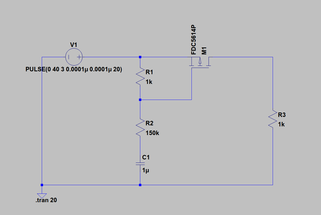
Here is a simple circuit with a P mosfet. I got a strange behavior when powering a circuit, so I isolated this part to understand it.

enter image description here

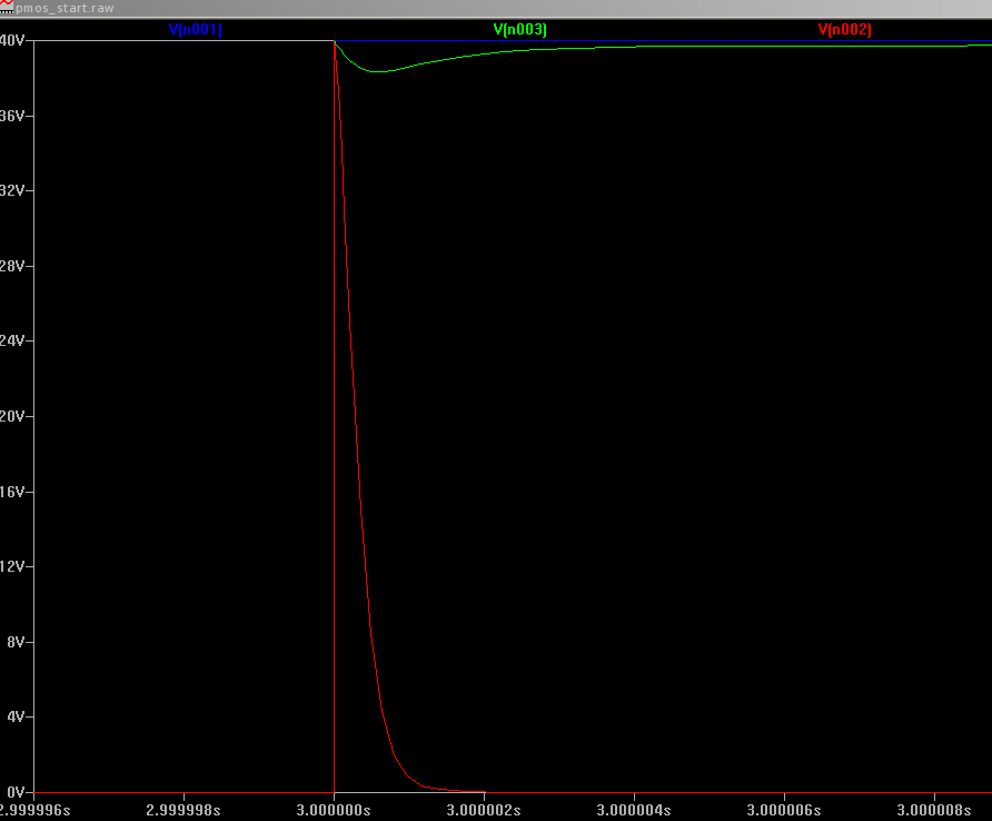
Circuit is powered at t = 3s (I've used a pulse input voltage source to simulate it). Here is a zoom on power on :

  • blue plot : input voltage
  • green plot : PMOS gate voltage
  • red plot : output voltage

enter image description here

As we can see, when circuit is powered on, during a transient phase of some µs, PMOS is closed. How can we explain that? Are some initial conditions missing in LTSpice simulation?

\$\endgroup\$

1 Answer 1

1
\$\begingroup\$

How can we explain that?

Actually it's the parasitic drain source capacitance that is inside the MOSFET that is producing the pulse at the output. Nothing really to do with conventional MOSFET action.

The FDC5614P has an internal capacitance of 90 pF and the CR time with R3 is 90 ns. At 5x CR the transient waveform should be pretty much over so that is a time of about 0.5 us and this looks about right on your graph given that you have a scale granularity of 2 us and my powers of interpolation aint that good!

Try shorting gate and source and removing C1 and R2 and repeat the experiment. I bet it looks very similar.

\$\endgroup\$
1
  • \$\begingroup\$ Many thanks for your explanation. I've confirmed in simulation that same behavior (but with different RC, in first case I get 40mV at 1.6µs, when gate shorted to source, I get 40mv at 2.1µs) can be observed when shorting gate and source and removing C1 and R2. \$\endgroup\$
    – rem
    Commented Jul 24, 2017 at 8:29

Your Answer

By clicking “Post Your Answer”, you agree to our terms of service and acknowledge you have read our privacy policy.

Not the answer you're looking for? Browse other questions tagged or ask your own question.