0
\$\begingroup\$

I am very new to FPGA programming. Got my Atlas DE0-Nano-SoC 5CSEMA4U23C5N board today and now trying to program the board using Quartus Prime Lite. Have created some VHDL code and run analysis and synthesis successfully, done the pin assignment and compiled and the programmer is picking up my device however when i add my output file and hit 'start' i just get "failed" in the progress bar. I suspect it has something to do with the configuration settings on the board. My university tutorial material mentions putting the switch with RUN and PROG on RUN however i have no idea what these switches are. (consultation of device manual didn't clarify this either.)

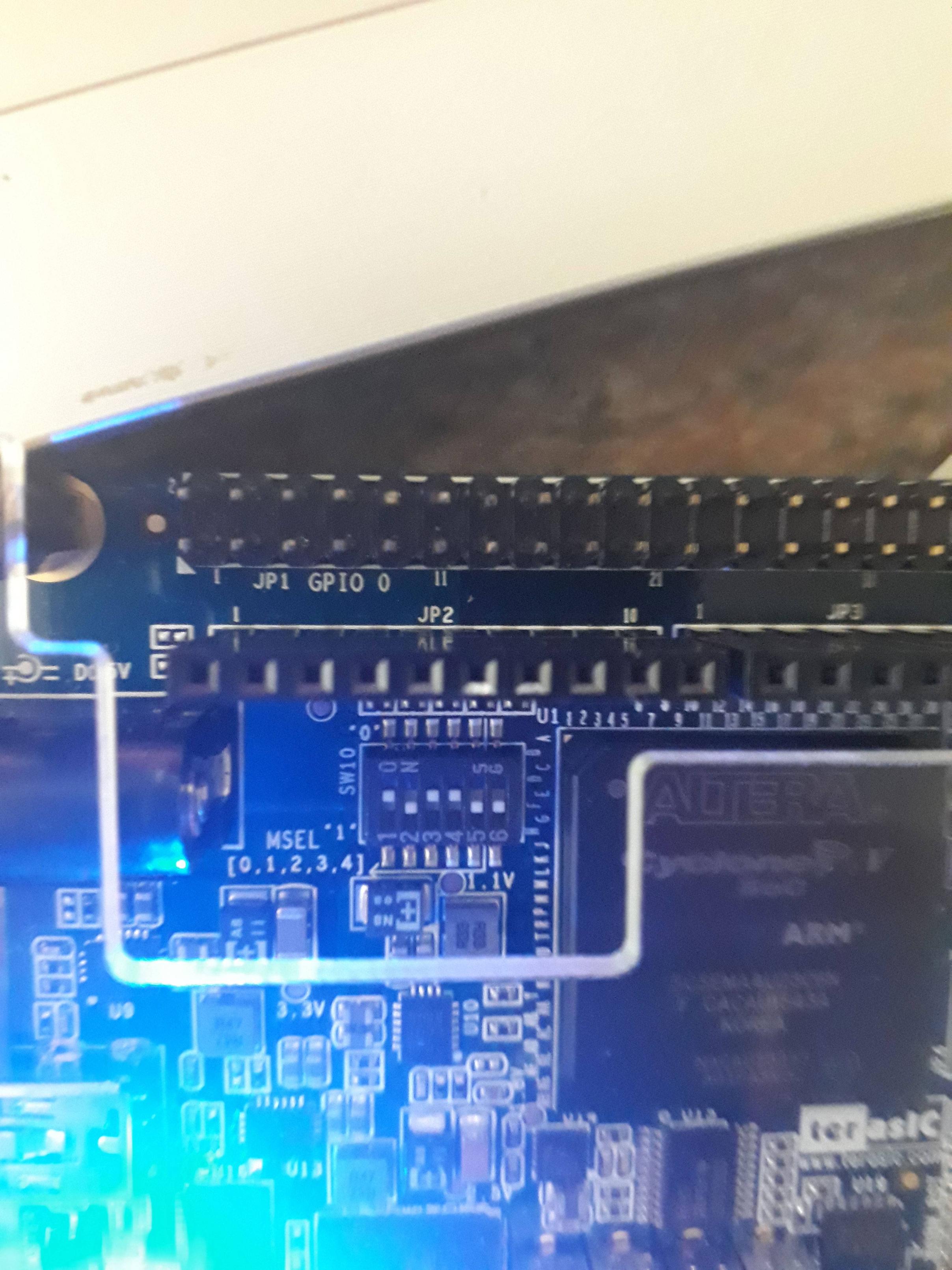
I currently have the configuration set to 1 up 2 down 3 up 4 up 5 down 6 down.

Could someone please explain what each switch does on the configuration and what it should be set to in order to put my program on the board. I am using Windows 10. Have put images of current configuration, code and the error below.

Board configuration

    library ieee;
    use ieee.std_logic_1164.all;

    entity FirstProject is
        port (  i1, i2  :   in  std_logic;
                o1      :   out std_logic);
    end FirstProject;

    architecture dataflow of FirstProject is 
    begin
        o1 <= i1 and i2;
    end dataflow;

enter image description here

\$\endgroup\$
3
  • \$\begingroup\$ Sorry, you expect us to debug something with no more information than an underlined box saying "Failed". Have a look at the system messages window and see what it actually says the reason for the failure was. \$\endgroup\$ Commented Aug 4, 2017 at 22:35
  • \$\begingroup\$ Does the JTAG chain in your programmer window have two devices (the FPGA and the SoC device)? If not click the "Auto Detect" button to scan the chain. Quartus won't automatically add the SoC to the JTAG chain when you launch the programmer so you will need to make sure it is there. \$\endgroup\$ Commented Aug 4, 2017 at 22:39
  • \$\begingroup\$ @TomCarpenter apologies, did not see the error pop up in the window. The error i get is " Error (209031): Device chain in Chain Description File does not match physical device chain -- expected 1 device(s) but found 2 device(s). " I tried the auto detect you suggested to add the FPGA to the chain. \$\endgroup\$
    – Blargian
    Commented Aug 5, 2017 at 4:05

1 Answer 1

0
\$\begingroup\$

The programing with JTAG can be done under any valid MSEL setting (the switch of the photo).

The MSEL setting specifies with way will be programmed automatically a FPGA at power-on (a download from EPCS Flash memory, or an upload by the boot software of the HPS-SoC part), and what configuration format is expected to be read (compressed/uncompressed, encrypted/unencrypted), what it is done with Quartus conversion tools.

at power-on, with way?
MSEL[4..0] 10010 (swith 1-6: ON OFF ON ON  OFF * ) from Flash, compressed/uncompressed
MSEL[4..0] 01010 (swith 1-6: ON OFF ON OFF ON  * ) from HPS software, compressed
MSEL[4..0] 01000 (swith 1-6: ON ON  ON OFF ON  * ) from HPS software, uncompressed
MSEL[4..0] etc

But JTAG works under any valid MSEL setting, so it is not related to your problem:

Try to start with JTAG programing from the beginning (without listed devices).

  1. Push in Hardware Setup button -> In Current selected Hardware select DE-SoC [USB-1], and Close the window.

  2. Push Autodetect, and at the emerging window select 5CSEMA4

  3. The autodetect will make appear two devices listed: SOCVHPS and 5CSEMA4 (Is this happening?)

  4. Select 5CSEMA4, right click -> Edit -> Change File

  5. Select the sof file generated by compilation, and push open. The name of the device 5CSEMA4 becomes 5CSEMA4U23.

  6. Select the Program/Configure checkbox placed at 5CSEMA4U23 Line.

  7. Push Start

In the step-4, if you did an Edit -> Add File, probably it altered the device chain in undesired way. I suspect this is what happened you.

With the above you put your program-configuration in the FPGA internal memory, not the EPCS Flash, so it will be temporal.

At future, when one desire to conserve the programing-configuration:

For upload the program-configuration to the Flash Memory, the sof file must be converted to a jic file, plus add to the above step-4 the EPCS128 device, where you will upload the jic file. The FPGA will read it at next power-on if the MSEL permit it (Or with a reset in boards designs what included it, it is not this case).

For store the program-configuration in the FAT partition of the SDCard, used by HPS SoC boot, the sof file must be converted to a rbf file (and the software booting process will upload it to the FPGA).

This means a 'HPS reset' will upload again the programing-configuration to the FPGA if the MSEL setting permit it, and that is why it is used usually the MSEL from Flash when one is testing and uploading with JTAG, as a 'just in case', or at least I see it this way.

\$\endgroup\$

Your Answer

By clicking “Post Your Answer”, you agree to our terms of service and acknowledge you have read our privacy policy.

Not the answer you're looking for? Browse other questions tagged or ask your own question.