Unfortunately, as is common for modules from Amazon, eBay, AliExpress etc., the technical info is limited. That is the "cost" you pay, for the low price :-( Often you need to do some reverse-engineering of the board yourself, if the vendor doesn't supply enough details.
I can't find a schematic for your module, and with the black solder resist, I can't see the PCB tracks well-enough on your photo, nor on the photos on the linked Amazon page. However the good news is that from other photos, it seems to be that:
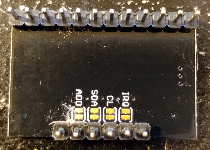
- The pair of gold-plated pads marked "ADD" are joined by a thin PCB track, by default.
- Then, the gold pad of that pair which is closest to the 6-pin 0.1" header, is connected to the pin in that header marked "ADD".
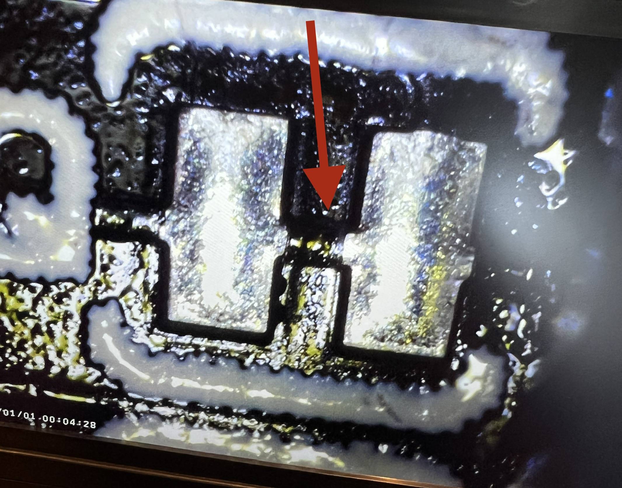
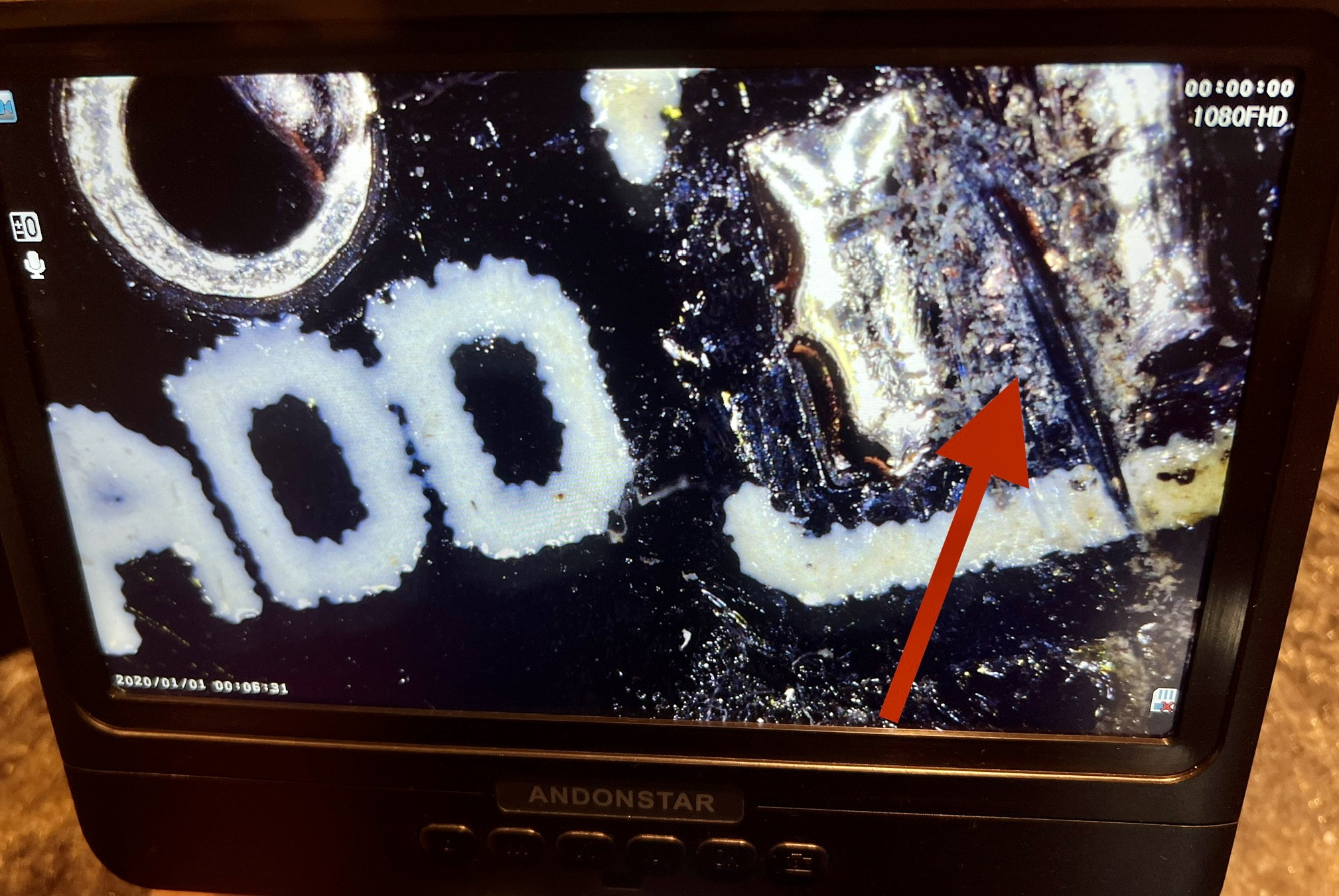
- I can't be sure exactly where you have cut, but you may have cut the track between that pad mentioned above, and the pin in that 6-pin 0.1" header for "ADD", thereby removing the chance to use the external "ADD" connection in that 6-pin header. :-(
Note that while this module refers to "ADD", the MPR121 datasheet refers to that signal as "ADDR".
If my assumptions above are correct, then in order to connect the "ADD" signal to one of the other documented options (to change the I²C address) you need to:
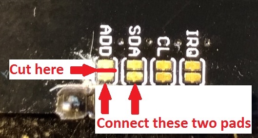
- Cut the (thin, almost invisible) track between the pair of gold-plated pads marked "ADD", using a scalpel blade etc. This disconnects the "ADD" signal from GND, which is the voltage on the gold-plated pad of the pair marked "ADD" that is furthest from the 6-pin 0.1" header (i.e. closer to the centre of the PCB)
- If you have not fully cut the track between the relevant 0.1" header pin and the closest gold-plated pad marked "ADD", then you can use that pin in the 6-pin header to connect to the "ADD" signal, after cutting the thin track between those pads.
- If you have cut that track between the 0.1" header pin and the closest gold-plated pad in the pair marked "ADD", then you either need to find a way to repair that break, or else solder a piece of thin wire (e.g. 30 AWG "wire wrap wire") to the gold pad of that pair closest to the 6-pin 0.1" header; then solder the other end of the wire to your selected choice, depending on which alternative I²C address you want (see the MPR121 datasheet). In my edited version of your photo, I have assumed that you will connect it to SDA.
Remember that I've reverse-engineered those connections from photos on Ebay and elsewhere just now. I can't guarantee that they apply to your module (although I expect that they do). If in doubt, you should trace the PCB connections on your module, as I mentioned at the beginning.
So to answer your questions in the order you asked (although I think I've covered all the points already above):
I see now on a product page it mentions the jumpers. I assume these are the pairs of contact pads on the back side?
Yes, although they would be better termed solder jumpers by the vendor.
So do I need to cut a trace in between the pair next to ADD
Yes, if you can see (or measure) a short between that pair of gold-plated pads marked "ADD".
and then connect ADD to say SDA with a wire?
That depends what you mean by "ADD". I believe you have cut the trace going to the "ADD" pin in the 6-pin 0.1" header, so you can't use the "ADD" pin in that header any more, if that is what you meant. In that case, the "ADD" connection you need to use, will be the one gold-plated pad of the pair marked "ADD" which is closest to the 0.1" header.
See my edited version of your photo below.
You should find that you can follow that track back to a through-hole "via" (between the middle "D" of "ADD" and the "D" of "SDA" on the silkscreen markings, as shown in your photo), where the signal then goes back to the MPR121 IC itself. If you scrape away enough of the solder resist on one side (or the other) of that "via", it will be a good place for using a multimeter to measure what is connected to the MPR121 "ADD" ("ADDR") signal.
In order to test that you can get a good connection to the "ADD" signal at that "via", after scraping away the solder resist, check for continuity between that "via" and the one gold-plated pad of the pair marked "ADD" which is closest to the 6-pin 0.1" header.
Update: Here is an edited version of your photo, summarising my suggested actions, assuming that:
- You have cut the track leading to the "ADD" pin in the 6-pin header (so you can't use that pin).
- You want to connect the "ADD" signal to "SDA" to select the 0x5C I²C address.
