Generally, is there any suggestion for multilayer PCB drill pairs that is practically possible to fabricate and has the minimum limits for traveling between layers and also has the minimum impact on price increment?
Yes. For these goals, use through vias only. This is possible to fabricate and will in fact have the lowest cost of any via technology. It allows electrical connections between any two layers, meaning it doesn't restrict layer connections at all.
Your other choices include, roughly in order of increasing cost:
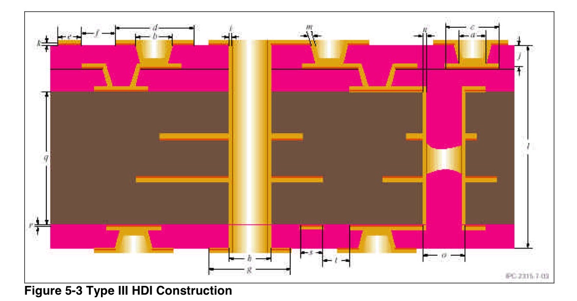
Through vias with back-drilling aka controlled-depth drilling: This means after through vias are drilled and plated, the board is returned to the drill machine and some portion of the via is drilled out again to remove the plating. This is used to reduce the capacitive parasitic for high speed traces. It does not improve the possible density of the board because the vias still take up space on all layers. The layers to be connected by the back-drilled vias cannot be in the region drilled out by the back-drill.
Sequential lamination: This means making up different sub-assemblies of the board (for example, in an 8-layer board, layers 1-4 might be in one sub-assembly, and 5-8 in another sub-assembly). Then each sub-assembly is drilled and plated. Finally the sub-assemblies are laminated together to make the completed board. This can improve signal integrity and improve board density, because the drills in one sub-assembly don't take up space in the other sub-assembly.
Micro-vias: This means vias drilled from either the top or bottom of the board through (typically) just the first one or two layers of dielectric. Often these are laser-drilled, but they can also be mechanically drilled. With laser drilling, they can be very small (.04 - .08 mm). This can improve both signal integrity and board density, compared to through vias. Micro-vias are commonly used beneath fine pitch BGA devices to achieve a reasonable break-out pattern. Micro vias can also combined with sequential lamination to achieve (for example) connections between layers 2 and 3 without impacting routing on other layers.
Usually any of these technologies is used in addition to, rather than as a replacement for, through vias.
Using any of these additional via technologies adds manufacturing steps (often both drilling and plating steps) and increases board cost, compared to just using through vias.
You should consult your fabrication shop for design rules and manufacturability recommendations before using any of these technologies.
Is it possible to make a VIA starting from 1st layer to 3rd layer and also from 1st to 4th without any consideration? If not possible, what is the best way to connect these layers?
Yes, a through via can connect these layers.
If you need to increase the density, you could also use sequential lamination or micro-vias.
Micro-vias are limited in aspect ratio (height to diameter ratio) and this generally limits them to layer 1-2 or maybe 1-3 connections (and typically requires using a very thin dielectric, maybe .08-.16 mm, between those layers). Using micro-vias would be facilitated if you changed your stackup to have signal on layers 1, 2, 5, 6 and power and ground on 3 and 4. With the thin layers used, it would not likely degrade signal integrity much to have return path on layer 3 for the signals on layer 1.

