0
\$\begingroup\$

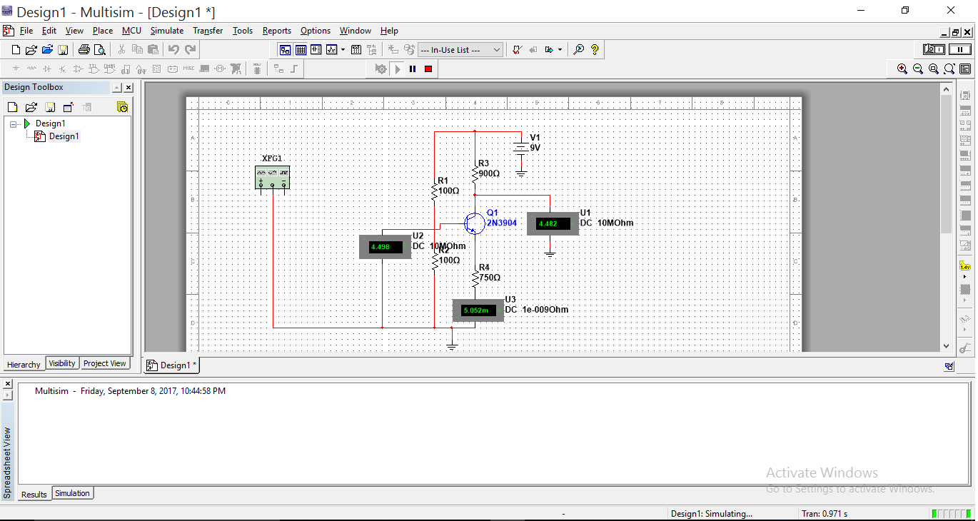
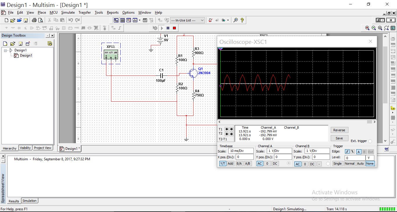
why the output of the Amplifier is distorted?

  1. the input from the function generator is 1 Vp
  2. the amplifier is baised at collector voltage of 4.5 V
  3. the frequency of the input signal is 1 khz
  4. the cutoff frequency of the input RC is 31.8 hz
  5. gain is about 1.2

i should get ~1.2v distortionless output
my circuit DC analysis

\$\endgroup\$
13
  • 1
    \$\begingroup\$ Because the design of your circuit is wrong. R1,R2 too low, Vb too high, RE too high, Q point ? \$\endgroup\$ Commented Sep 8, 2017 at 19:36
  • \$\begingroup\$ what is the effect of the low input impedance here ? Q point is Vc=4.5V and Ic=5ma \$\endgroup\$
    – user156489
    Commented Sep 8, 2017 at 19:40
  • \$\begingroup\$ There is no DC path to bias the base, as the tiny dot between base and R1R2 is missing. \$\endgroup\$ Commented Sep 8, 2017 at 19:43
  • \$\begingroup\$ no its connected i check it again it just does not show in the picture i dont know why @VladimirCravero \$\endgroup\$
    – user156489
    Commented Sep 8, 2017 at 19:46
  • 1
    \$\begingroup\$ Note that the Thevenin voltage for your base bias is ALSO 4.5V, which is a very bad idea. Your transistor is already close to saturation with no input signal. When the base is driven more positive, the transistor saturates, and you in fact end of driving the input signal itself directly through to the output via the B-C junction of the transistor! \$\endgroup\$
    – Dave Tweed
    Commented Sep 8, 2017 at 19:50

1 Answer 1

5
\$\begingroup\$

When constructing a low-gain amplifier like this, you need to pay attention to the voltage swing at both the emitter and collector of the transistor.

Let's say that you want to maintain a minimum voltage of 500 mV across the transistor in order to keep it from saturating. This means that the remaining 8.5V of your power supply will be distributed as 4.64V across the collector resistor and 3.86V across the emitter resistor.

This means that the collector can swing at most from 9V - 4.64V = +4.36V (minimum, near saturation) to 9V (maximum, near cutoff). Therefore, you want to set your Q point to close to the middle of this range (about 6.68V) in order to maximize the available signal swing.

This corresponds to an emitter voltage of 1.93V at the Q point, so you should design a bias network that has a Thevenin equivalent voltage of about 2.58V (VE + 650 mV).

\$\endgroup\$

Your Answer

By clicking “Post Your Answer”, you agree to our terms of service and acknowledge you have read our privacy policy.