From time to time I hear (and read) that it is not good to make separate Gnd planes for digital and analog circuit parts. It's all summarized in this rule of thumb: "Don't split the Gnd plane, don't make gaps in it." Usually this comes without clear explanation.
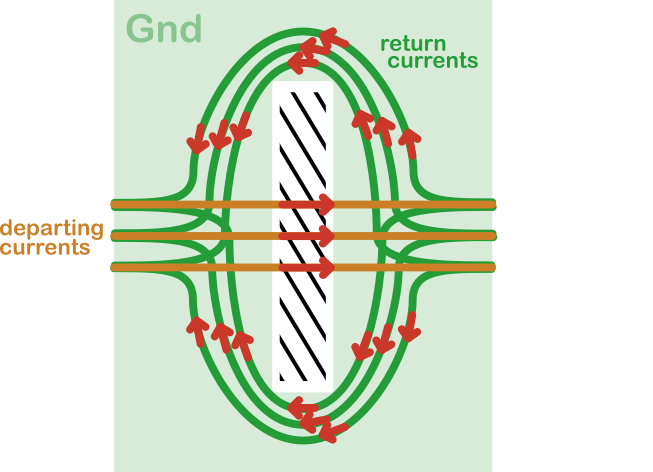
The closest I got to an explanation is this link: http://www.hottconsultants.com/techtips/tips-slots.html . The author points out that return currents will bend around the gap, such that the surface areas of the currents get large (borders of that surface area are defined by 'departing' and 'returning' current):
The return currents of the different signals are squeezed together at the corners of the gap, leading to cross-talk. The larger surface area of the current loops will emit and pick up EMC.
So far, so good. I do understand that no signals should be routed over such gap. Presuming you keep that rule in mind, would it still be bad to make gaps in the Gnd plane (eg. making a split between analog and digital circuit parts)?

