7
\$\begingroup\$

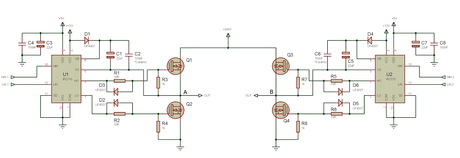
I've been working on an induction heater over the last few months and have had varied success. I can drive about 600W through it but as I begin to push past this point it isn't long until one of the FETs explodes. Below is the circuit schematic I based my driver on and the physical setup itself.

Reference schematic - circuit is based on this

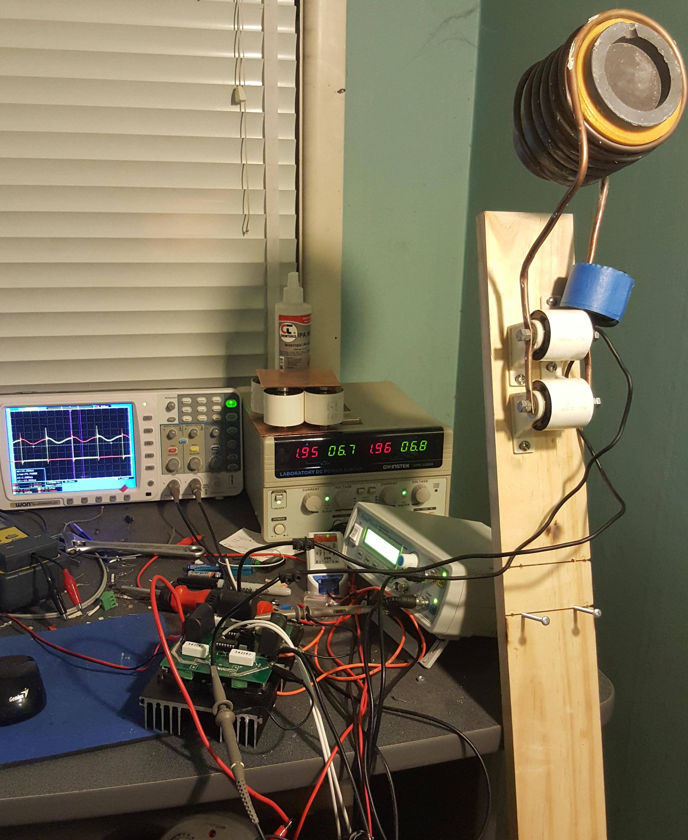
Physical setup

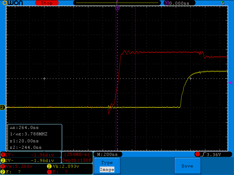
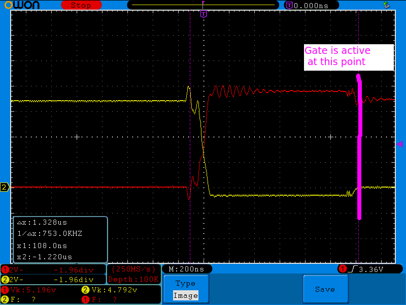
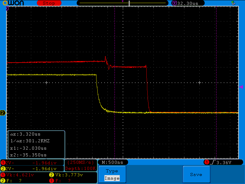
One of the issues that seems to plague the circuit is that each arm of the H bridge appears to switch on prematurely; the voltage at either node A or B will rise to the level of the DC bus prior to the high side gate being driven high. I've included a couple of waveform captures to help illustrate this. The first image shows the input to the high side gate (yellow) versus the output of node A (red). The second shows the 'precharge' that occurs between node A and node B.

i.stack.imgur.com/4rju2.png

i.stack.imgur.com/CWb7r.png

Currently the circuit is driven with a PWM waveform at 15.34KHz, 48% duty cycle. Q1 & Q4 are switched on simultaneously followed by a short dwell period to prevent shoot through and then Q2 & Q3 are driven simultaneously followed by another dwell period, repeatedly. The dwell period isn't apparent due to the 'precharge' that appears on either node. I'm trying to understand why this precharge is occurring and what I can do to resolve it. I suspect whatever may be causing it is creating other issues such as ringing etc.

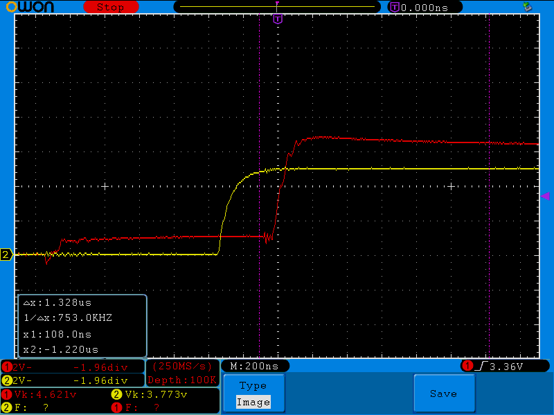
I had thought of increasing the duty cycle of the low side drivers to 50% while retaining the original duty cycle of the high side drivers in the hope of draining any residual charge, but this requires four PWM inputs which I don't currently have available and I'm not sure this is the solution to the problem. I've also tried using a 1uF capacitor as a snubber between one of the nodes and ground, I've found it does partially correct the issue but realistically just delays the effect until that arm discharges itself. You can see the effect below. The yellow signal is the logic reference.

i.stack.imgur.com/GRxBU.png

Here you can see the effect 'pushed' onto the end of the waveform.

i.stack.imgur.com/u7GwS.png

Apologies for the direct image links, SE is quite restrictive. Can anyone help me identify what is causing this 'precharge' effect?

\$\endgroup\$
9
  • \$\begingroup\$ What are the resistor R3-4 and R7-8 for? IR2110 outputs are not meant for resistive loads... \$\endgroup\$
    – next-hack
    Commented Sep 24, 2017 at 14:25
  • \$\begingroup\$ @Junkers: SE does limit the number of images in a post until the user has some rep. I've embedded them for you and given you some rep. \$\endgroup\$
    – Transistor
    Commented Sep 24, 2017 at 14:31
  • \$\begingroup\$ My implementation of this circuit doesn't include R3-4 and R7-8. I didn't really see the point of them and they didn't make any practical impact during simulation. \$\endgroup\$
    – Junkers
    Commented Sep 24, 2017 at 14:33
  • \$\begingroup\$ Which MOSFET did you use for Q1-4 ? \$\endgroup\$
    – next-hack
    Commented Sep 24, 2017 at 14:36
  • 2
    \$\begingroup\$ What is the frequency of your tank circuit (parallel I see). Operating frequency needs to be above resonant frequency of the tank circuit at all times. \$\endgroup\$
    – Marla
    Commented Sep 24, 2017 at 14:37

2 Answers 2

3
\$\begingroup\$

Did you know that FET stands for Fire Emitting Transistor?

I'm joking of course, but it sure seems true sometimes, doesn't it? MOSFETs, especially when juggling a lot of watts, can fail for the strangest reasons.

Magnetically induced EMF is not one of those reasons. The other answer seems to inexplicably be relating something with 2000A of current to a 600W 30A low frequency circuit, and makes a lot of other incorrect assumptions to get the 'result'. If this was a problem at such scales, switch mode power supplies, which have even <10 ns slewrates and can operate in the MHz, not KHz, at hundreds of amps, would simply not work. However, they do work.

Anyway, I believe your problem is a lesser-known quirk of MOSFETs called self-turn-on or phantom turn-on. This can happen when a MOSFET is subjected to a high dV/dT across it's source and drain - which is exactly what your circuit is doing. You generally never experience this issue until you start switching pretty big voltages (which, at 300V, you definitely are!).

In fact, you CAN see your dwell time in the chart you posted - specifically, the shoot-through condition begins about when the dwell time begins. This is because it really starts when the other leg of the h-bridge is turning off.

This subjects a huge dV/dT discontinuity, via the coil, to the low-side off MOSFET just before it is to turn on (simply because you are intending to turn it on shortly after the other H-Bridge leg has turned off). This voltage slams against the drain, and is actually able to couple into the gate via the mosfet's miller capacitance (the gate-to-drain capacitance). This causes current to flow through the gate-to-source resistor, which in turn results in a gate-to-source voltage. If you aren't careful about how you drive your gate, and especially at high voltages across the source and drain, you it can become significant enough to turn on the MOSFET. Normally, this usually only causes a shoot-through 'blip' that will erode efficiency/make your FETs get toastier than they should, but at 300V?

Yeah, they probably explode and quite impressively as well! Poor little transistors.

This is almost certainly caused by those 1K resistors you have across the gate to source. I would not relay on the UF4007 diodes to provide a quick discharge path through the IRF2110, especially when it's coupling capacitively like this. I would remove the 1K 'pull down' resistors on the gates entirely, and add a small capacitor from the gate to source instead (this will prevent the MOSFETs from accidentally turning on as well, but without any risk of phantom turn-on). I would also significantly reduce the gate resistor size. To 5Ω or even just remove them - most modern mosfets have a couple Ω of gate resistance anyway, making external gate resistors redundant. You're already OK with turning off the MOSFET hard with that diode, so I don't see much reason for using the gate resistors in the first place. Sure, this results in more EMI...but you're literally trying to emit EMI with an induction heater. Of all the possible projects, this one least of all needs a resistor slowing down the turn on of your MOSFETs. EMI is, ahem, not exactly a big concern given what else is going on here.

Basically, \$V_{gs}=R_{g}\cdot C_{gd}\frac{dV}{dT}\$

Here is a great app note on this (maybe Tahmid will read it too and update his schematics heh). Warning: Downloads PDF

\$\endgroup\$
1
  • \$\begingroup\$ I managed to solve this. I replaced the MOSFETs with newer trench stop IGBTs and voila, the issue is now gone. I suspect you're right about the miller capacitance. I could see a spike from the gate waveform on the output nodes with 0V DC across the bridge, indicating some form of coupling. \$\endgroup\$
    – Junkers
    Commented Jan 18, 2018 at 6:44
0
\$\begingroup\$

At 100 volts peak or 200volts PeakPeak, or 200/2.828 ~~ 60 volts RMS, for 600 watts you have 10amps RMS or 30 amps PeakPeak. The risetime of 100 nanoseconds provides a slewrate of 300 amps per microsecond. This produces intense magnetic field all around your PCB and +100v power leads (I see no bypass caps, to stabilize that +100 volts) and output "sin" waveform (through those 2 thick black wires running to the big capacitors).

Can you trust what the scope shows you?

Vinduce = [MUo * MUr * Area/(2 * pi * Distance)] * dI/dT

which we re-arrange to find

Vinduce = 2e-7 * Area/Distance * dI/dT

Now assume loop area is 0.1meter * 0.1 meter (4" by 4"); have lots of those in your circuit.

Assume distance is 0.1meter (either between wires and loops in your circuit, or between wires and the loop of your scopeprobe/GNDwire).

What voltage is induced? I don't know yet. We must run the numbers.

Vinduce = 2e-7 * 0.1m * 0.1m / 0.1m * 300 e+6

Vinduce = 2e-7 * 0.1 * 300 e+6 = 60 e-7 e+6 = 60e-1 = 6 volts.

Thus your current surges induce 6 volts into any 4" by 4" region of your PCB+wiring. Or perhaps 12v, because of "S" shape of typical risetime waveforms.

Do your control circuitry tolerate injected 6 volts, or 12 volts, atop any of the waveforms.

You should expect a 12 volt artifact imposed on any waveform, unless your probing methods are real-good, real low-area. Note this is at 4" distance.

And that high-frequency gate ringing? At 20MHz. What path supports that? For 20MHz, the Luh*Cpf is 25,330/(20 * 20) = 25,330/400 = 60 Luh*Cpf. At 10nH, C will be 6,000pF.

Years ago, I was asked to consult on a flawed speed controller for a rock crusher. Management/marketing wanted to improve the human-factors of the controlcab, and less room was available for the electronics (some installations will upgrade if "new" fits easily into "old" spaces in the rock plants.)

But the "new" had field failures. Occasionally. Turned out the embedded-system programmer had moved the control-electronics (for gate control of IGBTs) closer to the 500 amp (or was it 1,000 amps, or 2,000 amps bus-bar-plate) and some of the MOSFET drivers were failing, eventually). Some of the MOSFET drivers never failed, and some (positions on the PCB) were 80% of the failures. Thus we had a position-on-PCB-related field-failure situation. I used that same formula Vinduce = 2e-7 * Area/Distance * dI/dT to compute Vinduce.

In that situation, Vinduce was just a bit higher than 6 volts. I had the (local) field-rep craft a 25mm by 25mm (1" by 1") loop at end of coax, and go look for injected voltages. Couple weeks passed, and in the next phone-conversation, the consultant admitted he and the field-rep had seen/screen-grab voltages of 1.5 volts right against the PCB. I never knew whether the "against the PCB" was on the side-exposed-to-500ampere (2,000 amperes?) or on the side-shielded-by-PCB-chopped-up-planes.

How can 1.5 volts be a problem? Because 1.5 volts is right in the forbidden region for logic signals, and circuits are upset, with unknown state, when a metastable voltage appears.

\$\endgroup\$
1
  • \$\begingroup\$ You make some valid points but I don't believe induced EMF is my problem here. I did some more probing around and found that even with 0V DC across h bridge I can see elements of this precharge waveform appearing at the outputs. I think my issue may be related to the Miller capacitance of the mosfets but I'm not quite sure how to rectify this. \$\endgroup\$
    – Junkers
    Commented Oct 8, 2017 at 1:11

Your Answer

By clicking “Post Your Answer”, you agree to our terms of service and acknowledge you have read our privacy policy.

Not the answer you're looking for? Browse other questions tagged or ask your own question.