1
\$\begingroup\$

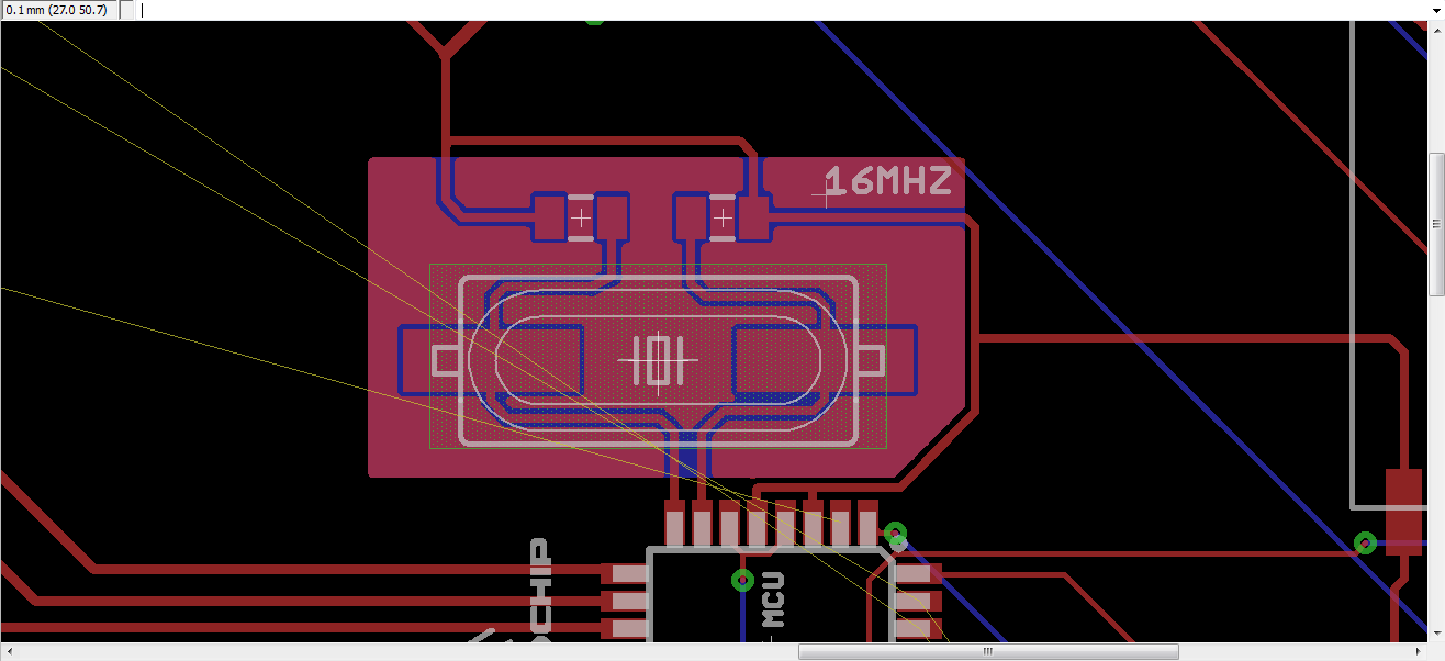
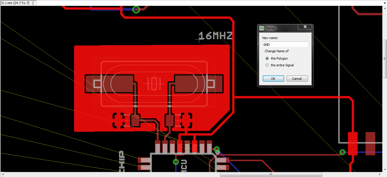
I'm designing an Atmega328P-AU based WiFi development board for my school project, and as you know, crystal oscillators may take some effort to layout, especially when we have a WiFi module. I've been reading AVR PCB LAYOUT for OSCILLATORS practice file, but I still don't know if my design is correct. Any advice or suggestion is appreciated!

enter image description here

EDIT 1: Just renamed the top plate as GND: enter image description here
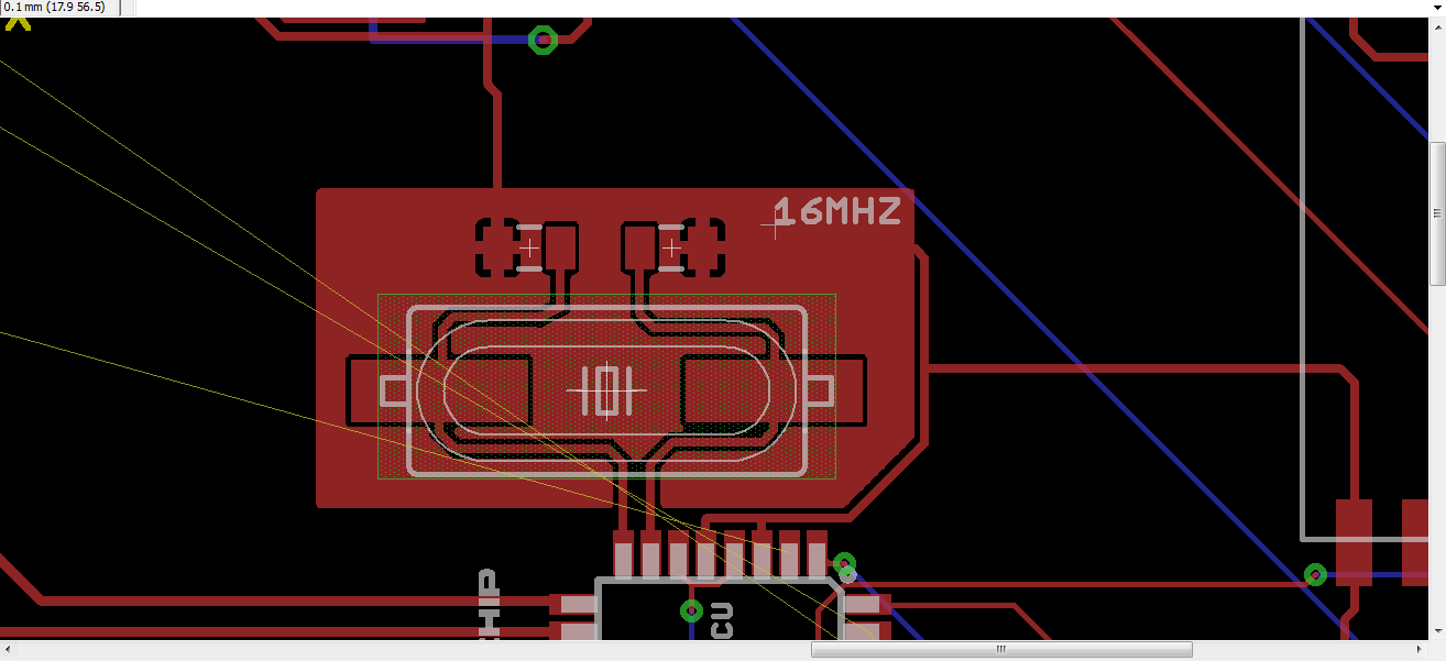
EDIT 2: Changed capacitor's position: enter image description here
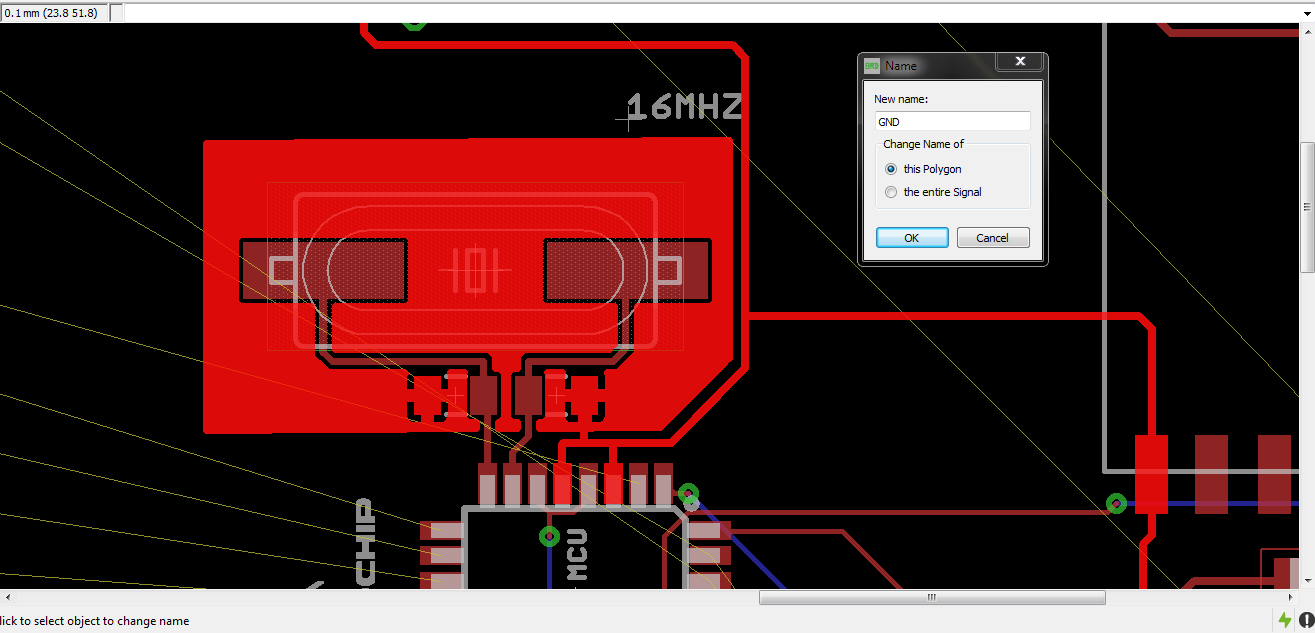
EDIT 3: Reduced length of wire that connects XTAL1 and XTAL2 to MCU enter image description here
\$\endgroup\$
7
  • 2
    \$\begingroup\$ The fill is not grounded. \$\endgroup\$ Commented Nov 4, 2017 at 12:12
  • \$\begingroup\$ What do you mean with fill? \$\endgroup\$ Commented Nov 4, 2017 at 12:16
  • \$\begingroup\$ crystal oscillators may take some effort to layout No idea where you get that "wisdom" from, as far as I know Crystal oscillator layout is quite straightforward. But as Ignacio pointed out, you made big WHOOPSIE by not making that plane connect to ground. You should also remove the ground traces connecting to the 2 capacitors and just connect them to the ground plane. It is only 16 MHz so I do not see what is so difficult/troublesome about the layout. \$\endgroup\$ Commented Nov 4, 2017 at 12:17
  • \$\begingroup\$ We mean the area that surrounds all the components, make that grounded. I suggest that you look at some existing designs and see "how it is done". So crack open almost any device like a broken DVD player for example. There is almost no device these days that does not have a crystal oscillator inside. Then just copy that. There is no point in inventing this all new by yourself. \$\endgroup\$ Commented Nov 4, 2017 at 12:19
  • \$\begingroup\$ I'll try to elaborate on the problem they are pointing out. Make use of your planes, they have lower inductances than your trace. At 16 MHz it matters, so you are making relatively large loops, for no reason. In reality it may work but be very sensitive to noise, worst case scenario => you put your finger on the PCB and the noise from (you as an antenna with mains), then perhaps... it will stop oscillating. Who knows. It's like pumping your bicycle tires with water. It may... work... but... it's not good. \$\endgroup\$ Commented Nov 4, 2017 at 12:29

2 Answers 2

3
\$\begingroup\$

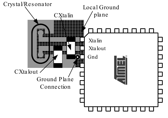
Amin, Figure 1-1 in the AVR186: Best Practices for the PCB Layout of Oscillators you linked in your question gives this layout recommendation:

AVR186 1-1

Why do you do it differently? Your layout has the caps behind unnecessarily long tracks, which adds inductivity and diminishes the effect of the caps. It may even introduce weird oscillation modes of the crystal.

Please place the caps between the µC and the crystal and keep the tracks as short and wide as possible. Also, use a guard ring (local ground plane) around the crystal which is connected to ground only by one single thick lead near the µC. Do not connect other GNDs to that ring.

\$\endgroup\$
8
  • \$\begingroup\$ which pin of the atmega328p-au is XTAL IN? \$\endgroup\$ Commented Nov 4, 2017 at 13:22
  • \$\begingroup\$ XTAL1 is the input, XTAL2 is the output. This information is in the datasheet, section 9.3. Please see the datasheets as your reference, always. A lot of good men d̶i̶e̶d̶ nearly died to make these. \$\endgroup\$
    – Janka
    Commented Nov 4, 2017 at 13:40
  • \$\begingroup\$ I changed the position of the capacitors and added a GND polygon around the crystal \$\endgroup\$ Commented Nov 4, 2017 at 13:59
  • \$\begingroup\$ Not good, because the inductivity of the GND path to the output cap is still high. \$\endgroup\$
    – Janka
    Commented Nov 4, 2017 at 14:06
  • \$\begingroup\$ I don't know what you mean..... \$\endgroup\$ Commented Nov 4, 2017 at 14:28
3
\$\begingroup\$

The ground fill improves susceptibility but if it also couples input and output signal across crystal then it reduces gain margin so the gap to tracks should increase.

Load capacitors should be low leakage and stable across temperature (NPO or COG type)

  • The load capacitors should be placed close to each other
  • The load XTAL IN capacitor should be placed first and closest to the XTAL IN pin and ground
  • Parasitic capacitance will reduce gain margin. Keep this to an absolute minimum. For example typically: – XTAL IN to ground: 1pF – XTAL OUT to ground: 2pF

  • XTAL IN to XTAL OUT : 0.5pF ( on a good design.)

    • These values are slightly package dependent.
    • Reduce the parasitic capacitance between XTAL IN and XTAL OUT pins by routing them as far apart as possible
    • A ground area should be placed under the crystal oscillator area. This ground land should be connected to the oscillator ground.
    • Connect the external capacitors needed for the crystal and the ceramic resonator operation as well as the crystal housing to the ground plane
    • In case there is only one PCB layer, it is recommended to place a guard ring around the oscillator components and to connect it to the oscillator ground pin
\$\endgroup\$

Your Answer

By clicking “Post Your Answer”, you agree to our terms of service and acknowledge you have read our privacy policy.

Not the answer you're looking for? Browse other questions tagged or ask your own question.