0
\$\begingroup\$

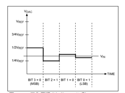
Many picture of SAR ADC blocks from the internet show that the output of SAR logic is the output of the SAR ADC, but I also found that lots of papers show the output by using the \$V_{DAC output} \$ and the \$V_{in}\$ ,like the picture below.

enter image description here

So I am a little confused now: is the output of SAR ADC equal to the output of SAR logic, and the value of SAR Logic output equal to the \$V_{DAC output} \$, and the \$V_{DAC output} \$ must be approximate the \$V_{in}\$ ?

\$\endgroup\$

1 Answer 1

0
\$\begingroup\$

The SAR uses a S&H (Sample and Hold circuit) on the input and then successively compared with the voltage for that bit starting from most significant which equals full scale/2.

If the input is less than this reference ( i.e. comparator output =0) that bit must be a 0 and if positive that held values is next offset by that bit analog voltage.

After offset is applied and the difference settles and is sampled and the same comparator output is sampled and if negative or "0" output then there is no change to the approximation and if positive then another offset for that bit voltage is applied . This repeats until all the bits have been compared whether it is a 8 bit SAR or a 12 bit SAR etc.

Hence the name Successive Approximation Register (SAR).


My attempt to explain how they work without specifying hardware type.

  1. Sample and Hold input and buffer going into n bit SAR
  2. Subtract Vref/2^n (DAC out switch voltage) from Vin
  3. wait small time to stabilize signal
  4. Clock comparator output into shift register
  5. If output=1 then keep that DAC bit high to offset Vref/2^n (e.g 1/2,1/4,1/8...*Vref)
  6. increment n and repeat from 2. until done.
  7. result is stored in Shift Register. Output may be serial or parallel.
  8. Clear Register when done waiting for next trigger to start ADC.
\$\endgroup\$
4
  • 1
    \$\begingroup\$ So the output is? \$\endgroup\$
    – Shine Sun
    Commented Nov 19, 2017 at 0:55
  • \$\begingroup\$ The output is sampled on the comparator logic level output into a shift register on each successive approximation .. In this diagram, 0101... starting from most significant bit worth Vref/2 and next worth Vref/4 etc. so the DAC applies a correction voltage to the input to Approximate the voltage Since the input is below Vref/2 on the 1st comparison, MSB=0 The shift register is not shown. curtisma.org/wp-content/uploads/2014/01/… \$\endgroup\$
    – D.A.S.
    Commented Nov 19, 2017 at 1:36
  • \$\begingroup\$ ,So the output of sar adc is the output of comparator?really? \$\endgroup\$
    – Shine Sun
    Commented Nov 20, 2017 at 4:51
  • \$\begingroup\$ Yes the comparator output is clocked into a serial shift register to store the entire bit pattern from most significant to least. \$\endgroup\$
    – D.A.S.
    Commented Nov 20, 2017 at 22:54

Your Answer

By clicking “Post Your Answer”, you agree to our terms of service and acknowledge you have read our privacy policy.

Not the answer you're looking for? Browse other questions tagged or ask your own question.