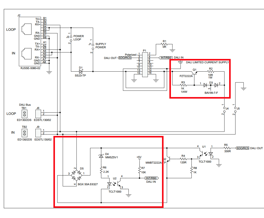
I am trying to understand how this schematic works. It is a physical layer implementation of the DALI specification. The schematic is in this document (page 11). I have mainly two questions:
In reception mode: when the bus is idle (voltage level between 9.5 and 22.5 V, according to the specification) if the lower limit (9.5V) is analyzed, the current through the optocoupler diode is: $$\frac{V_\text{bus (idle)}-V_\text{f (bridfe)}-V_\text{Z (D4)}-V_\text{f (U2)}}{R_6} = \frac{9.5-0.7- 5.1-1.25}{2.2\,\text K} = 1.1\text{ mA}$$ (approximately). With such current value, the U2 optocoupler transistor is not saturated and therefore, DALI_IN is not close to 0 V.
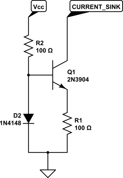
What am I analyzing erroneously? For \$V_\text{bus(idle)}=22.5\,\text V\$, the current is approximately 7 mA, so DALI_IN has a voltage close to 0 V (the transistor is saturated).Limited current source: The DALI specification limits the maximum current to 250 mA. In the schematic, the limited current source is created with Q1, D3, R2 and R3 but I can not understand how it works. How are the maximum current value and the output voltage calculated?


