4
\$\begingroup\$

Updated based on feedback with better screenshots (I hope) - I am also working on getting the files onto a file sharing site so they can be accessed at full resolution

I am really confused about the attached LTSpice circuit behavior

LTSpice circuit

The voltage source V2 is simply a 5V supply and Voltage source V1 is a square wave of 40us period (5 volts)

I run the simulation - with the 5V square wave I would expect the Q1_Collector voltage to drop to 0 within 500ns of Q2 collector voltage going to 5 volts however the Q2_Collector voltage does not drop to 0 for 3us and I am trying to understand why.

On the plot show below - I am plotting collector voltages at net Q2_Collector - in Green and voltages at Q1_Collector in purple - The cursors show how when the Q2_Collector voltage rises to 5Volts the Q1_Collector voltage does not switch off for almost 3us

Ltspice plot

I see from the data sheet that Q1 has a switch off time of 70ns and a storag time of 70~100ns. I created the circuit to model the switch off times and I noticed that the turn off times I observe in the simulation are of the order of microseconds (2-3) microseconds to be precise.

I also built a circuit to see if what I was observing was a simulation issue but the circuit showed a similar behavior - infact I saw switch off times of almost 6us.

My question - can someone please help me understand why I am seeing such a difference between what I would expect from the Datasheet? Obviously I am doing something wrong and just cannot get what.

I am working on posting links to the files if these are still not very clear.

\$\endgroup\$
3
  • 3
    \$\begingroup\$ Three things that would help: Make the schematic big enough to read. Label the nodes that you plotted so we know what the graph is showing. Make the graph using colors we can read (the dark blue is almost unreadable). \$\endgroup\$
    – The Photon
    Commented Jul 2, 2012 at 21:49
  • \$\begingroup\$ What The Photon mentioned and make a small description about what you're doing, what you expect, and how the result differs. The sources (TRAN/PULSE) in the barely readable drawing are not very descriptive. Also include node numbers. The green line does remind me about the Miller platform a bit, but I doubt that can be it. \$\endgroup\$
    – jippie
    Commented Jul 2, 2012 at 21:53
  • \$\begingroup\$ I have attempted to update per the comments however I see it is still hard to make out the colors - wish the site allowed attachments - I will look for a file hosting site to post the screen shots \$\endgroup\$ Commented Jul 2, 2012 at 22:59

2 Answers 2

4
\$\begingroup\$

Have you tried replicating the test circuit from the 2N3906 datasheet, and seeing whether that matches your 1-2us results?

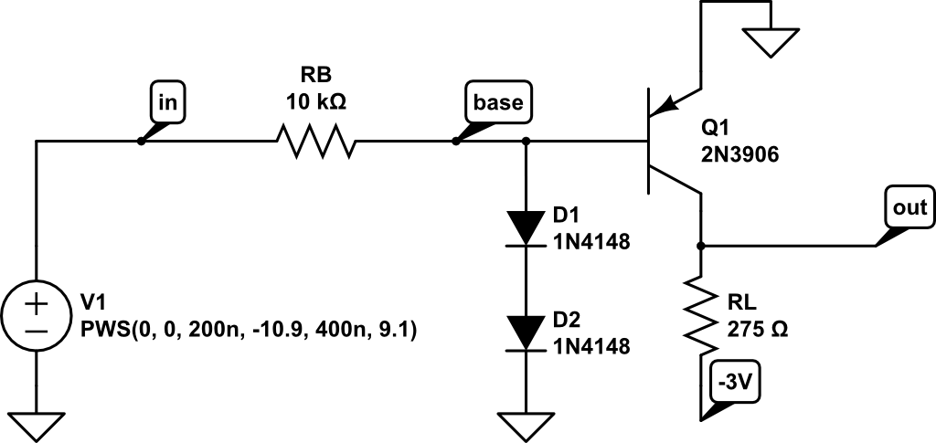
The test circuits for datasheet-quoted storage and turn-off times drive the base hard in reverse. In this datasheet, they drive the base-emitter junction to a 9V reverse bias through the 10K base resistor, so they basically go from 1mA out of the base (PNP forward bias) to 1mA into the base (PNP reverse bias). They do that "hard reverse" intentionally to extract the stored charge and get the BJT to shut off faster. If your circuit isn't so aggressive about it, the turn-off time will be a lot longer.

Here's a simulation you can run of the 2N3906 switching performance based on the datasheet circuit (click "open in editor", hit F5 to run sim):

BJT switching time schematic

BJT switching time voltages

BJT switching time currents

It takes about 80ns for Q1 to shut off (roughly from t=400ns to t=480ns), and that's with V1 pushing almost 1mA into the base (see the trace for "I(Q1.nB)"). If you change the piecewise-step source V1 to only go to 0 at 400ns, you'll find it takes far longer to shut off.

Also see the question "What is the reverse recovery time in a diode?".

\$\endgroup\$
1
  • \$\begingroup\$ like the circuitlab approach will look at using that for questions as it would be very convinient to collaboratively change things if needed. I think you are right the specs on the 3906 pretty much dictate the behavior I am sseing I tried with a mmbt3940 and switching times are much better \$\endgroup\$ Commented Jul 3, 2012 at 16:34
2
\$\begingroup\$

Sounds like the base-collector capacitance is being effectively multiplied by the 2N3906's gain. Google "Miller effect" for more on that phenomenon. There don't seem to be any time constants that could account for a delay that long, unless you take the beta into account.

\$\endgroup\$

Your Answer

By clicking “Post Your Answer”, you agree to our terms of service and acknowledge you have read our privacy policy.

Not the answer you're looking for? Browse other questions tagged or ask your own question.