A very old heater unit at work broke down so we replaced one of its ~50 controller boards. All the boards are the same.
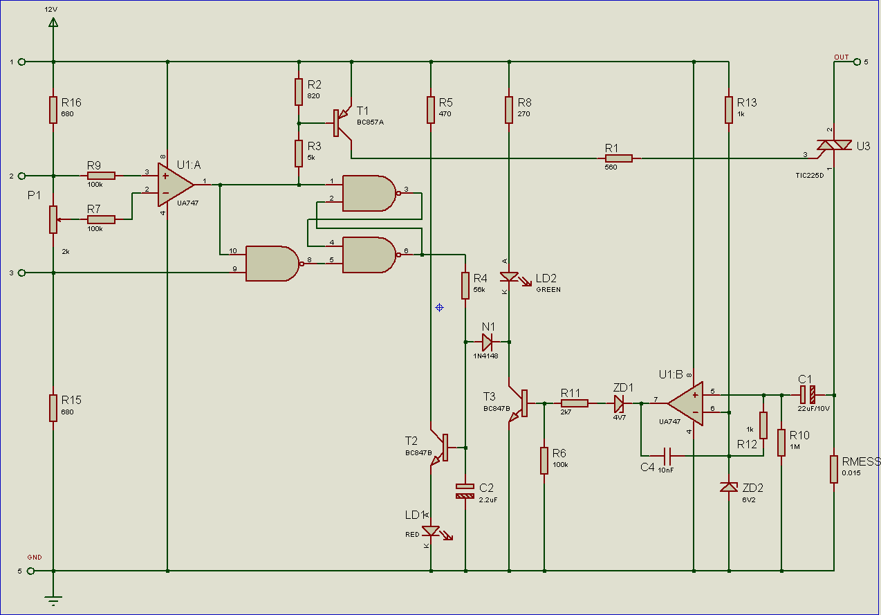
Just for the sake of practise electronics, I asked if I could take the board home and play with it. The 74LS00 was completely burned out, but the rest was intact so I was able to make a schematic out of it. See attached image.
What I want to do now is try to get a hunch of what each part / block / area of the schematic does.
There are five terminals on the board (1-5). 1 (top-left) = +12V input, 4 (top-right) = output, 5 (bottom-left) = ground. I do not know what signal 2 and 3 are other than the fact that the board is marked with a square wave beneath pin 2, and a sawtooth beneath pin 3. Obviously these are some kind of signals from the heater unit.
"Analysis" I've done so far:
I have not worked much with opamps before, but what I can see on U1:A is that it does not have any feedback loop, just two inputs. Therefore I surmise that this opamp is running in a comparator setup, although I have no clue what R9 and R7 does. Are these some kind of noise filters?
The two right-most NAND-gates is an R/S-latch, that I can see, so when pin 3 is high and the opamp is high, left-lower NAND gives a zero to R, and the opamp gives 1 to S. This must mean, I think, that for any other combination of opamp + pin 3 the R/S is reset. Opamp + pin 3 = set.
If U1:A is high it must also mean T1-base does not have any bias. I'm guessing this because R2-top = 12V and R3-bottom = 12V, meaning T1-base = 12V, meaning it's cut-off. T1 cut-off means TRIAC U3 is cut-off, so no output on pin 4.
This is what I've found so far, even if it doesn't give me even half the picture. I have no idea what U1:B does, but since Rmess = 15mohm my best guess is that Rmess is a shunt resistor. C1+R10, if that's an RC-filter, perhaps U1:B is measuring the current over Rmess?
LD1 and LD2 are obviously status indicators. R4+C2 RC-filter for T2, if R/S-latch is set then it's an error? If I understand correctly, this would mean, following my deduction above, that U1:A and pin 3 can not be high at the same time.
These are just fair guesses, but I'm really curious about the purpose of U1:B because of its negative feedback which I cannot figure out.
So, question: What does U1:B do here?

