3
\$\begingroup\$

I would like to provide an external input digital signal to a Xilinx Basys 3 FPGA PMOD GPIO pin. Since the board is powered with 3,3V, I think I need to supply a LVTTL signal. However, I would like to use the TTL output of a NI-USB-6008 board to drive the input of the FPGA. From the NI-USB-6008 I read that the TTL output is LVTTL and CMOS compatible. Is it safe to directly interface the NI-USB-6008 output to the FPGA input pin? Or is it better to generate a 0V - 3,3 V analog output from the NI-USB-6008 to couple directly with the FPGA? Thanks for your replies!


Thanks for the detailed reply. I will implement a buffer as suggested. However, this triggers another question, mainly for curiosity: why the solution that uses the analog output of the NI-USB set to 0 - 3,3V board to interface with the LVTTL of the FPGA should be avoided? Could that possibly erogate too much current and damage to components of the FPGA inputs, or is more elated to a loss in performances in the digital signal level-transition speed?

\$\endgroup\$
4
  • 1
    \$\begingroup\$ You probably don't want an analog output. First thing you should do is read the actual digital output voltage specifications of the NI board - not the name of the signalling type, but the actual voltages. Then compare with the FPGA allowances. \$\endgroup\$ Commented Mar 28, 2018 at 17:05
  • 1
    \$\begingroup\$ Using that analog output sounds like a bad idea, unless you know exactly what the output will produce (for example is it a true DC level, or is a series of PWM pulses of higher voltage that average to the requested one) and also what it could produce if erroneously mis-configured by buggy software. Also it's probably slower than a digital output, and might spend time at forbidden intermediate levels. \$\endgroup\$ Commented Mar 29, 2018 at 18:44
  • \$\begingroup\$ Thanks Chris for all these details. As you can see, I'm quite new to the field and probably too "naive". And unfortunately I have limited access to equipments, that's why I'm trying to get the best I can with what I have. In any case, I've tested with an oscilloscope the "analog" output of the board, that is a 0-5V continuous DC level. At this point I guess what I need is prevent errors from programming and check what happens in intermediate levels. A problem that -- correct me if I'm wrong -- may appear also using faster digital level switches, but for a shorter amount of time. \$\endgroup\$
    – Valerio
    Commented Mar 31, 2018 at 8:02
  • \$\begingroup\$ Using the analog output really sounds like a bad idea. Wherever possible, try to design systems which are electrically safe regardless of what the programmer does. For the kind of performance you can likely achieve with the analog out, this could be as simple as two resistors per signal - surely you can source those? \$\endgroup\$ Commented Mar 31, 2018 at 17:05

1 Answer 1

3
\$\begingroup\$

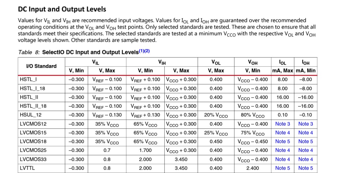
Basys3 IOs are either LVCMOS/LVTTL (2.5 to 3.3 V). Refer datasheet.http://www.xilinx.com/support/documentation/data_sheets/ds181_Artix_7_Data_Sheet.pdf enter image description here It would be unsafe to use 5V TTL to drive them. Use voltage translators/buffers.

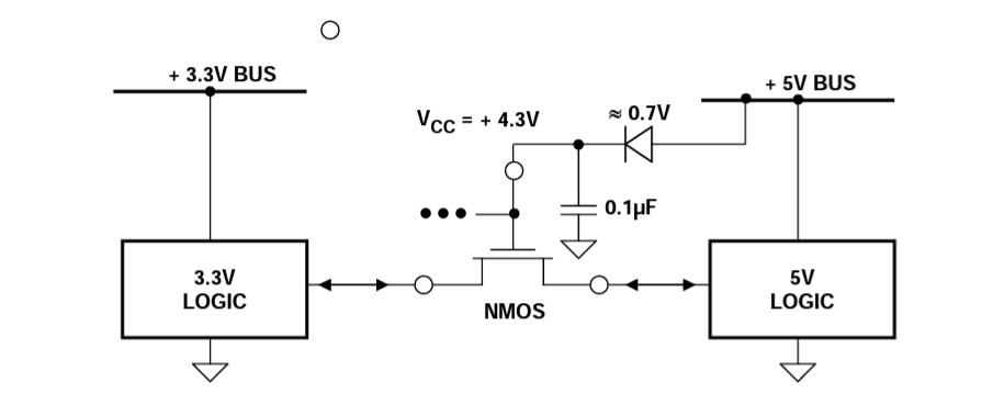
A simple way of translation between 3.3V -- 5V enter image description here

\$\endgroup\$
0

Your Answer

By clicking “Post Your Answer”, you agree to our terms of service and acknowledge you have read our privacy policy.

Not the answer you're looking for? Browse other questions tagged or ask your own question.